Continue to Site

Welcome to EDAboard.com

Welcome to our site! EDAboard.com is an international Electronics Discussion Forum focused on EDA software, circuits, schematics, books, theory, papers, asic, pld, 8051, DSP, Network, RF, Analog Design, PCB, Service Manuals... and a whole lot more! To participate you need to register. Registration is free. Click here to register now.

Self oscillating flyback converter

Status
Not open for further replies.

anditechnovire

Newbie level 6
Joined
Jun 22, 2020
Messages
12
Helped
0
Reputation
0
Reaction score
0
Trophy points
1
Activity points
92
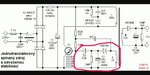
Please how does this simple self oscillating flyback converter work, and also regulate it output.
Most importantly, the function of 1N4148, ZD5v6 and c2(i.e. all the base component) please.


iz_odv.png
 
Last edited by a moderator:

The diode symbols are wrong in several places!
Basically, the AC feedback path is through the lower 4n7 capacitor and 220R resistor.
The voltage from the feedback winding is rectified by the 1N4148 and charges C2. Note it is wired to produce a negative voltage. When the voltage reaches about 5.6V, the Zener diode starts to conduct and the bias is drawn away from the transistor, reducing the current in the transformer primary and hence the output voltage.
This kind of regulation isn't very precise because it can't compensate for the actual output voltage, only an approximately proportional version of it in the feedback winding. Losses in the transformer and output rectifier and changes in the load are only partially compensated.

Brian.
I really appreciate your response. Infact this response has triggered questions from how the original circuit works.

Here I only understand that a small current flows through the 330k resistor to the base of the transistor, to initiate the turn on process. As the transistor is partially ON(active region), collector current will flow and energize the primary winding, as a result, a same polarity voltage will be induce in the feedback winding which will create a positive regenerative feedback and conduct more current to the base of the transistor, and the transistor turn on fully(saturation).
That's all I know. I don't know how the transistor will switch OFF. I might make some assumptions based on my knowledge of the joule thief circuit, but am not sure.
I don't also know how the RC circuit affect the switching frequency.
 

To me it looks like a blocking oscillator. Similar to how the joule thief operates.

1) 330k resistor slightly biases the transistor On.
2) Admitting current through winding #1.
3) Inducing current in winding 2.
4) Sending increased bias to transistor.
5) Current builds in winding 1, and plateaus.
6) Flux stops changing in transformer. Bias ceases from winding 2.
6) Shutting off the transistor, or nearly off.
 
as drawn, when it turns on, the 4n7 gives a burst of current to the base of T1, helping it turn on fully, the startup when C2 is uncharged is very messy, best to sim on LT spice and examine waveforms ....
 
To me it looks like a blocking oscillator. Similar to how the joule thief operates.

1) 330k resistor slightly biases the transistor On.
2) Admitting current through winding #1.
3) Inducing current in winding 2.
4) Sending increased bias to transistor.
5) Current builds in winding 1, and plateaus.
6) Flux stops changing in transformer. Bias ceases from winding 2.
6) Shutting off the transistor, or nearly off.
So will the base winding have to reverse it polarity, or will the transistor have to be forced out of saturation?
 

The diode symbols are wrong in several places!
Basically, the AC feedback path is through the lower 4n7 capacitor and 220R resistor.
The voltage from the feedback winding is rectified by the 1N4148 and charges C2. Note it is wired to produce a negative voltage. When the voltage reaches about 5.6V, the Zener diode starts to conduct and the bias is drawn away from the transistor, reducing the current in the transformer primary and hence the output voltage.
This kind of regulation isn't very precise because it can't compensate for the actual output voltage, only an approximately proportional version of it in the feedback winding. Losses in the transformer and output rectifier and changes in the load are only partially compensated.

Brian.
Please does the feedback rectifier conduct when the transistor is off?
 

So will the base winding have to reverse it polarity, or will the transistor have to be forced out of saturation?

Perhaps reverse polarity occurs at some point, because one description says the transistor is exposed to ringing and/or negative voltage. This causes a need for a way to protect it. (Your schematic has a network of diodes and capacitors which could be for that purpose.)

However apart from that, the theory of shutoff in winding #2 is that it stops generating bias current due to winding #1 reaching its DC current limit. Which is to say AC is no longer in the transformer, and a transformer works on AC.
 

the xtor turns off when it can no longer support the peaking current in the Tx, thus the voltage on the bias wdg collapses ( and then reverses ) helping turn of xtor T1, with the aid of C1 (when it is fully charged ) - it is not a flash ckt ...
 

the xtor turns off when it can no longer support the peaking current in the Tx, thus the voltage on the bias wdg collapses ( and then reverses ) helping turn of xtor T1, with the aid of C1 (when it is fully charged ) - it is not a flash ckt ...
Ok thanks.
Please do you have any idea on the regulation circuit. I mean this part.
 

Attachments

  • 1593103452401.jpg
    1593103452401.jpg
    17.5 KB · Views: 542

When C2, the 10uF 16V cap gets to about 5v6 plus a wee bit it tends to hold the main xtor off, the coils supplies 5v6 + 0.6 volts on the 4148 to charge the cap, this is about 6.2V on this wdg, for the 7;15 ratio on the Tx the output will see 15/7 * 6.2 = 13.28 less the o/p diode drop, say 0.8 volt under load = 12.5 volt ( higher at no load ).
There is no current limiting and not very good regulation of Vout with load - it is a ckt that can fail easily - esp at start up due to high currents in the main transistor ...
 

None of UF4007, BA159, UF5004 and 1N4148 are Schottky types.
The symbols for the 1N4007 input rectifiers are correct.

Brian.
 

When C2, the 10uF 16V cap gets to about 5v6 plus a wee bit it tends to hold the main xtor off, the coils supplies 5v6 + 0.6 volts on the 4148 to charge the cap, this is about 6.2V on this wdg, for the 7;15 ratio on the Tx the output will see 15/7 * 6.2 = 13.28 less the o/p diode drop, say 0.8 volt under load = 12.5 volt ( higher at no load ).
There is no current limiting and not very good regulation of Vout with load - it is a ckt that can fail easily - esp at start up due to high currents in the main transistor ...
Ok, I get that.
Please what will determine the amount of voltage induced in the feedback winding?
And if there was no kind of regulation, how how will the output voltage look like? (cause while I was experimenting, without any regulation. The output voltage increased as much as possible rather than obeying the principle of turns ratio).
 

the voltage in any wdg on a flyback, goes up, at fet turn off, until limited by the clamping action of connected circuits - in this case there a re two - the o/p diode and cap ( and load ) and the feedback diode and cap ( and its 330 ohm load ) ...
 

the voltage in any wdg on a flyback, goes up, at fet turn off, until limited by the clamping action of connected circuits - in this case there a re two - the o/p diode and cap ( and load ) and the feedback diode and cap ( and its 330 ohm load ) ...
Ok I kinda get you, but please you need to understand that am quite a novice, in this area.
So you mean that if the value of the capacitor is 12v then the induced voltage will increase to 12v.
Is that what you're saying? Or will the diode and load also be included?

Please I'll really appreciate it if you could give any example(if available).
According to my understanding of joule thief, when the fet or transistor is off, the magnet field will collapse, and voltage will be induced in the opposite direction which will increase to the point where current can flow in the load(LED). So in this case of rcc flyback where there is no led, it really making me confused.
 

No, what is being said is the output would not stabilize unless there was a load. In a Joule Thief, the LED is the load, in your schematic, it is the 330 Ohm resistor across the output. If you remove it, the spikes in secondary voltage will make it rise much higher.

There is no output voltage stabilization at all in the circuit, it relies upon the feedback winding picking up the same signal, although not necessarily the same voltage as the output winding. If one produces more voltage, so will the other. When the rectified feedback voltage exceeds the Zener diode breakdown voltage it 'strangles' the transistor and limits the current it can pass and hence reduces the output. When running it will try to reach an equilibrium point where the transistor is conducting just enough that the Zener holds it back. Under increased load, there will be less voltage on the feedback winding so the Zebner will conduct less and the transistor will switch harder.

A much better system is not to monitor the feedback winding but to monitor the real output voltage, that way the losses in the transformer and rectifier are also taken into account. The problem that introduces is that the secondary is no longer isolated from the AC lines so it poses a risk of electric shock. That is why you will see an opto-coupler in most small power supplies of this kind. The output voltage is converted to current on the input side of the optocoupler (LED side) and its output side goes to the switching transistor. It works like the 1N4148 and Zener diode in your schematic
 

where current can flow in the load(LED). So in this case of rcc flyback where there is no led, it really making me confused.

The led acts just like a freewheeling diode connected across the winding, as the flux collapses.

In a flyback the secondary performs similar (freewheeling) action, as the flux collapses.
 

Status
Not open for further replies.

Similar threads

Part and Inventory Search

Welcome to EDABoard.com

Sponsor

Back
Top