gahelton
Newbie level 4
I'm sorry, but I'm about at my wits end. I have been trying to create clocks for an FPGA design so that I can verify timing constraints.
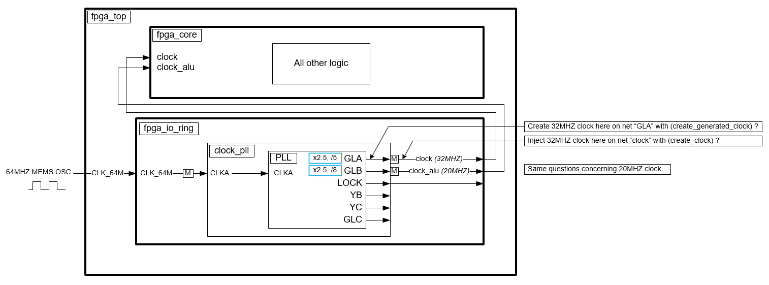
I've tried some many iterations and followed examples with very limited success. Below is a block diagram for my system.
Ultimately, I need to create a clock (32MHZ) to inject into FPGA signal "clock", and a clock (20MHZ) to inject into FPGA signal "clock_alu", both for the purpose of verifying time constraints.

====================================================
This is my latest iteration of the portion of the SDC file that is supposed to create these clocks. I am not as concerned about the uFROM_CLOCK right now.
====================================================
Looking at the clock summary from the log file
It appears as if "clock" and "clock_alu" are being created, but they are not being assigned to the proper port/pin/net in the design. Instead, the tool is "inferring" the GLA and GLB clocks out of the PLL, and are not using the clocks that I've defined.
I've tried using get_ports, get_pins, I've tried using absolute paths like fpga_core_1/fpga_io_ring_1/clock_pll_1/pll/GLA -or- fpga_core_1.fpga_io_ring_1.clock_pll_1.pll.GLA.
I've also tried versions without the instance numbers like fpga_core.fpga_io_ring. etc, etc.
If tried variant after variant, with no success so far.
=========================================================
Also, at one point, I had a line in the SDC file that said that "clock" and "clock_alu" were async to each other, and not to check timing between them, but I have lost it along the way.
Any help would be greatly appreciated.
Thanks
I've tried some many iterations and followed examples with very limited success. Below is a block diagram for my system.
Ultimately, I need to create a clock (32MHZ) to inject into FPGA signal "clock", and a clock (20MHZ) to inject into FPGA signal "clock_alu", both for the purpose of verifying time constraints.
====================================================
This is my latest iteration of the portion of the SDC file that is supposed to create these clocks. I am not as concerned about the uFROM_CLOCK right now.
Code:
set sdc_version 1.7
set_time_format -unit ns -decimal_places 6

########  Clock Constraints  ########

create_clock -name { CLK_64M }  -period 15.625000 [ get_ports CLK_64M ]
create_clock -name { clock } -period 31.250000 [ get_pins { clock_pll/GLA } ]
create_clock -name { clock_alu } -period 41.666667 [ get_pins clock_pll/GLB } ]


create_clock  -name { uFROM_CLOCK } -period 100.000 -waveform { 0.000 50.000  }  { \
fpga_core_1/inst_ufrom_interface1/reg_ufrom_clock:Q }Looking at the clock summary from the log file
========================================================Clock Summary
*****************
Start Requested Requested Clock Clock Clock
Clock Frequency Period Type Group Load
---------------------------------------------------------------------------------------------------------------------
CLK_64M 64.0 MHz 15.625 declared default_clkgroup 0
System 32.0 MHz 31.250 system system_clkgroup 230
clock 32.0 MHz 31.250 declared default_clkgroup 0
clock_alu 24.0 MHz 41.667 declared default_clkgroup 0
clock_pll|GLA_inferred_clock 32.0 MHz 31.250 inferred Inferred_clkgroup_1 6264
clock_pll|GLB_inferred_clock 32.0 MHz 31.250 inferred Inferred_clkgroup_2 1170
uFROM_CLOCK 10.0 MHz 100.000 declared default_clkgroup 0
ufrom_interface|ufrom_clock_inferred_clock 32.0 MHz 31.250 inferred Inferred_clkgroup_0 72
=====================================================================================================================
@W:MT532 : breu_fpga_io_ring.vhdl(665) | Found signal identified as System clock which controls 230 sequential elements including fpga_io_ring_1.EEPROM_SI_1. Using this clock, which has no specified timing constraint, can adversely impact design performance.
@W:MT530 : ufrom_config.vhd(53) | Found inferred clock ufrom_interface|ufrom_clock_inferred_clock which controls 72 sequential elements including fpga_core_1.ufrom_interface_1.ufrom_config_1.UFROM0. This clock has no specified timing constraint which may adversely impact design performance.
@W:MT530 : breu_fpga_io_ring.vhdl(474) | Found inferred clock clock_pll|GLA_inferred_clock which controls 6264 sequential elements including fpga_io_ring_1.timer_1ms_counter[14:0]. This clock has no specified timing constraint which may adversely impact design performance.
@W:MT530 : addition.vhdl(94) | Found inferred clock clock_pll|GLB_inferred_clock which controls 1170 sequential elements including fpga_core_1.servo_controller_1.position_tracker_1.alu_1.addition_1.c_i[32:0]. This clock has no specified timing constraint which may adversely impact design performance.
It appears as if "clock" and "clock_alu" are being created, but they are not being assigned to the proper port/pin/net in the design. Instead, the tool is "inferring" the GLA and GLB clocks out of the PLL, and are not using the clocks that I've defined.
I've tried using get_ports, get_pins, I've tried using absolute paths like fpga_core_1/fpga_io_ring_1/clock_pll_1/pll/GLA -or- fpga_core_1.fpga_io_ring_1.clock_pll_1.pll.GLA.
I've also tried versions without the instance numbers like fpga_core.fpga_io_ring. etc, etc.
If tried variant after variant, with no success so far.
=========================================================
Also, at one point, I had a line in the SDC file that said that "clock" and "clock_alu" were async to each other, and not to check timing between them, but I have lost it along the way.
Any help would be greatly appreciated.
Thanks
Last edited by a moderator: