Continue to Site

Welcome to EDAboard.com

Welcome to our site! EDAboard.com is an international Electronics Discussion Forum focused on EDA software, circuits, schematics, books, theory, papers, asic, pld, 8051, DSP, Network, RF, Analog Design, PCB, Service Manuals... and a whole lot more! To participate you need to register. Registration is free. Click here to register now.

Schematic diagram from Verilog code

Status
Not open for further replies.

David83

Advanced Member level 1
Joined
Jan 21, 2011
Messages
410
Helped
45
Reputation
92
Reaction score
45
Trophy points
1,308
Activity points
3,639
Hello all,

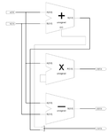
How can I draw the schematics of my RTL verilog code. Something like the attached figure. I use ModelSim to write and simulate my design. Does it support this? Also, is finding such schematic is the synthesis process itself or it's something different?

Thanks
 

Attachments

  • Schematic.png
    Schematic.png
    137.9 KB · Views: 323

Various tools have different levels for this. For Vivado, you can get a schematic after each step of the design.

The first being elaboration, the second being synthesis, and the last being implementation. There are small differences between each of these steps as they work at different levels of abstraction.

The tools will take the RTL and first map language constructs into general blocks it knows how to implement. eg, muxes, comparators, adders, adder-trees, fsms, memories, etc... The results after implementation will show the basic elements used to construct these muxes, comparators, etc...

As you enable more synthesis and implementation optimizations, the resulting schematic will look less and less like the human-readable version you have.
 

Thanks again.

Is synthesis done by a third person (one writes the RTL code, one who does the verification, and one who does the synthesis), or it's a part of one of the other two persons' part? I'm asking this question because I would like to be a hardware designer, and I'm not sure if I need to go to synthesis, or just focus on the RTL code and verify it tentatively using testbenches?

You probably want to ask this question in the ASIC forum. As I've mentioned, some companies focus more on ASICs or on FPGAs, and others have a part-time guru for such task.

There also isn't just synthesis. There is implementation. Synthesis is taking RTL and finding things that look like stuff. Implementation is taking stuff and actually putting it on a FPGA/ASIC.

More specifically, there is a difference between deciding a Verilog source wants an adder-tree, and finding an ideal implementation of that adder-tree.
 
I downloaded Vivado and did the simulation of a simple 1-bit half adder using behavioral description as

Code:
always @(A,B)
begin
if (A==B)
S=1'b0;
else
S=1'b1;
end

always @(A,B)
begin
if (A&B)
C=1'b1;
else
C=1'b0;
end

where A and B are the inputs, and S and C are the sum and the carry on bits. The simulation works fine by testing it using a testbench.

Now, in synthesis, what I'm looking for exactly? I watched a video on YouTube, and the presenter said that we need to run implementation, which automatically runs synthesis first. After that he looked for the report timing summary (Path delay type=max, Report unconstrained paths is checked. What are these?) Then we go to unconstrained path option, and select setup to view the net delays and logic delays and the total path delays.

Then I went to the synthesis option, and selected the Schematic option, and gave me the attached schematic. Does this mean that my code is unsynthesizable? Because I have two blocks not defined using logic gates. These could be Look up tables, but in the summary it says that I have only 1 LUT and 4 I/O. By the way, what are IBUF, and OBUF?

In short, after successful simulations, what are the important things I should check/know?

Thanks
 

Attachments

  • schematic.pdf
    10 KB · Views: 249

OK, I found it. It was under RTL Analysis ---> Elaboration Design --->schematic. In this case I get the details of my design; in logic gates, comparison operator, ...etc. It's attached. But why in Synthesis I got a look up table? Finally, implementation I get only report summaries about delays, power consumption, .. etc, right?
 

Attachments

  • schematic1.pdf
    10.7 KB · Views: 139

The "basic elements" of a technology are the circuits the tools will use to implement your logic. In ASICs, the basic elements will be and/or/etc... gates as well as any custom-designed structures that have been optimized by hand.

FPGAs are based on lookup tables -- small ROMs, as well as fast carry chains and a few other bits of logic.
 
Status
Not open for further replies.

Part and Inventory Search

Welcome to EDABoard.com

Sponsor

Back
Top