Atif Hussain Shah
Member level 1
Hi,
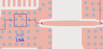
I am Simulating LNA S2P file in ADS using Cosimulation method. The results are in accordance with datasheet when i use ideal ground( Global schematic ground) but when i use circuit ground(local ground)the results are not good. What could be the reason?
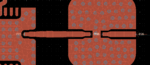
I want to simulate the effects of local ground which will be the real practical situation.
I am Simulating LNA S2P file in ADS using Cosimulation method. The results are in accordance with datasheet when i use ideal ground( Global schematic ground) but when i use circuit ground(local ground)the results are not good. What could be the reason?
I want to simulate the effects of local ground which will be the real practical situation.
Attachments
-
 S2P With Ideal Ground(Global Schematic Ground).PNG79.8 KB · Views: 202
 -
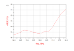 Input Return Loss With Ideal Ground(Global Schematic Ground).PNG16.5 KB · Views: 143
 -
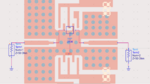 S2P With Circuit Ground(local Ground).PNG81.2 KB · Views: 211
 -
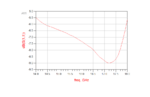 Input Return Loss With Circuit Ground(local Ground).PNG19 KB · Views: 201
 -
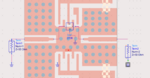
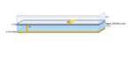 Substrate definition.PNG12.2 KB · Views: 208