esm.
Junior Member level 3
Hello all.
I have a good knowledge on RS-485 buses. I have some doubts about the internal fail-safe feature of MAX487.
I know how to do a fail-safe biasing using external pull-up and pull-down resistors, but my doubt is just about the internal fail-safe feature of these transceivers.
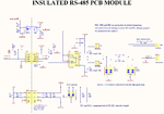
Currently I can't do tests in practice with my ICs (MAX487). I won't use a MAX485 because I could need more than 32 nodes attached to the RS485 bus (MAX487 supports up to 128 nodes).
When receiving at the RS485 bus, I know that:
VA-VB >= 200mV ---> RO pin is level '1'
VA-VB <= 200mV ---> RO pin is level '0'
VA-VB > 200mV && < 200mV ---> RO pin has undeterminated logic state
MAX487 / MAX485 datasheet says: The receiver input has a fail-safe feature that guarantees a logic-high output if the input is open circuit.
Considering the following condition:
1) Supply voltage = 5V
2) DE and RE pins at level '0' constantly (that means transmit is disabled and receive is enabled)
3) A and B pins left floating (No termination resistor and no fail-safe biasing external resistors connected). Nothing connected to both pins A and B
Questions
1) Does these RS485 tranceivers have an internal pull-up from pin A to VCC and a internal pull-down from pin B do GND? (with higher values?)
2) In this condition, what should be the voltage between A and B (5V)? (Considering a very high input impedance meter)
3) At question 2, the logic level at RO pin is '1', right?
4) Now, if I put just a termination resistor (120 Ohms) between A and B, the logic level at RO will be 'undeterminated', right? I think if the internal resistors are present, they will have a high value and the voltage between A and B will be near to 0V due to the low resistance of the termination.
I really have these doubts a long time.
Someone can help?
I have a good knowledge on RS-485 buses. I have some doubts about the internal fail-safe feature of MAX487.
I know how to do a fail-safe biasing using external pull-up and pull-down resistors, but my doubt is just about the internal fail-safe feature of these transceivers.
Currently I can't do tests in practice with my ICs (MAX487). I won't use a MAX485 because I could need more than 32 nodes attached to the RS485 bus (MAX487 supports up to 128 nodes).
When receiving at the RS485 bus, I know that:
VA-VB >= 200mV ---> RO pin is level '1'
VA-VB <= 200mV ---> RO pin is level '0'
VA-VB > 200mV && < 200mV ---> RO pin has undeterminated logic state
MAX487 / MAX485 datasheet says: The receiver input has a fail-safe feature that guarantees a logic-high output if the input is open circuit.
Considering the following condition:
1) Supply voltage = 5V
2) DE and RE pins at level '0' constantly (that means transmit is disabled and receive is enabled)
3) A and B pins left floating (No termination resistor and no fail-safe biasing external resistors connected). Nothing connected to both pins A and B
Questions
1) Does these RS485 tranceivers have an internal pull-up from pin A to VCC and a internal pull-down from pin B do GND? (with higher values?)
2) In this condition, what should be the voltage between A and B (5V)? (Considering a very high input impedance meter)
3) At question 2, the logic level at RO pin is '1', right?
4) Now, if I put just a termination resistor (120 Ohms) between A and B, the logic level at RO will be 'undeterminated', right? I think if the internal resistors are present, they will have a high value and the voltage between A and B will be near to 0V due to the low resistance of the termination.
I really have these doubts a long time.
Someone can help?