spman
Advanced Member level 4
Hello
I want to forward the clock of design (entered from a GCLK) to output of the FPGA(Spartan3).
When i use this code :
The post rout simulation gives x (unknown) for XClk ! i checked the FPGA Editor. the XClk net is directly routed from ClkIn Pin without passing from a BUFG. so i used this one:
but after implementation this warning is given :
help me please
thanks
I want to forward the clock of design (entered from a GCLK) to output of the FPGA(Spartan3).
When i use this code :
Code:
module Top(ClkIn, ..., XClk);
	input	ClkIn;
	output	XClk;

	assign	XClk = ClkIn;

	always	@(posedge ClkIn)
		...
endmodule
Code:
module Top(ClkIn, ..., XClk);
	input	ClkIn;
	output	XClk;

	wire	Clk;
	BUFG	BUFG_Ins(.I(ClkIn), .O(Clk));
	assign	XClk = Clk;

	always	@(posedge Clk)
		...
endmoduleand likewise the state of XClk in post route simulation is unknown!WARNING:Route:455 - CLK Net:XClk_OBUF may have excessive skew because 0 CLK pins and 1 NON_CLK pins failed to route using a CLK template.
help me please
thanks
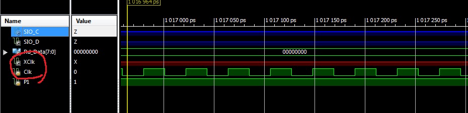
") In that screenshot I count about 7 Clk periods in 300 ps, so that's in the 23 GHz ballpark. I think you may have lost a factor of 1000 somewhere.
In that screenshot I count about 7 Clk periods in 300 ps, so that's in the 23 GHz ballpark. I think you may have lost a factor of 1000 somewhere.