Continue to Site

Welcome to EDAboard.com

Welcome to our site! EDAboard.com is an international Electronics Discussion Forum focused on EDA software, circuits, schematics, books, theory, papers, asic, pld, 8051, DSP, Network, RF, Analog Design, PCB, Service Manuals... and a whole lot more! To participate you need to register. Registration is free. Click here to register now.

RFID reader antenna with microstrip patch antenna

Status
Not open for further replies.

sanchez251

Newbie level 3
Joined
Apr 19, 2010
Messages
3
Helped
0
Reputation
0
Reaction score
0
Trophy points
1,281
Location
Germany
Activity points
1,316
Hello guys!

First I want to tell, that I like that site! It's very useful! Second, something about myself: I'm a student of a German technician school and now doing some kind of thesis about RFID. Please remember that I'm a newbe in designing and analizing antennas. Futher I'm sorry for my bad english...

Here is the problem:

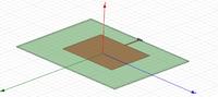
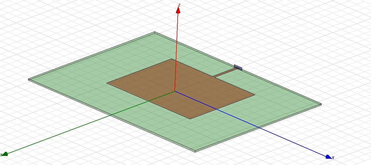
One Part of my thesis is to analyze and buid an antenna which works on 866 Mhz (I'm using EPC Gen1 Class2 Transponders EU). The antenna have to be very thin, because it have to lie on the floor ant read all transponders above. Because this I want to buid a microstrip patch antenna with 50 Ohm feed and using a PCB FR4 as substrate (Er = 4.4).

Here I found some help about developing the patch and the microstrip line:

https://www.emtalk.com/mscalc.php
https://www.emtalk.com/mpacalc.php

On basic of this tutorial ( https://www.emtalk.com/tut_1.htm ) I have adapted a existing example to my application. I simulated the patch antenna with HFSS (V10.0), but simulation has shown that the antenna isn't as good as i want. I also built a prototype of this antenna and measured the SWR. It is about 5!

I'll uppload the HFSS-File so you can test it for yourself. For everyone who don't have HFSS here are the dimensions:


f = 866 Mhz
FR4 1.52 mm
Er = 4.4

Patch:
W = 105.41 mm
L = 82.41 mm

Feed: (Have to be 50 Ohm)
W = 2.85 mm
L = 31.35 mm

Waveport:
H = 3 mm
W = 10 mm

What's wrong? Please can someone help me? THX!!!

Regards
Sanchez251
 

Hello Guys!

Is there someone who can help me, please?

Thank you very much!

Regards
Sanchez251
 

Hi..

I actually ran ur design on my HFSS because im also designing a patch RFID but with inset feed..

The antenna actually resonates at 882MHz..

ill say do a parametric sweep on the size of the patch and i read in some papers that increasing the size of the patch reduces ur resonance frequency so try that..

Added after 11 minutes:

Something else.. ur substrate height was 1.52 i guess.. which i find strange because FR4s of 4.4 are usually at 1.6.. if u change that ur S11 improves up to -30dB..

do that then do a parametric sweep.. and to do a parametric sweep u will need to draw the whole structure by using variables..

i would recommend using polylines..
 
Hello,

I assume the underside of the FR4 PCB is all metal? If so, this will not be a good antenna. As the current in the patch is counteracted by a same but opposite current in the image element. The image element is just 3mm below the driven element. So the produced far field per ampere current in the middle of the patch will be very low. If there were no losses, the useful bandwidth will be very low and the half wave patch resonator has very high Q factor.

By adding the lossy dielectric, all your input power will be dissipated into the dielectric. Check your radiation efficiency in the simulation (don't forget to enter dielectric loss for the FR4).

There is another thing, I assume that the 82mm size in x direction. Did you check the current distribution (use a display where you can also see the direction of current, for example a current animation)? The width is over 0.5 lambda electrically, so you may get a strange current distribution with current in the patch that produce counteracting far field.

When you need some performance, you need to increase the distance to the ground plane reduce the width so you get your main patch current in X-direction. This will yield several hundred ohms impedance when feeding at the edge.

You can feed via a quarter wave transformer or make cuts in the patch so the feedline runs somewhat into the patch to reach a point of lower impedance.

When it really must be flat, you need to remove the ground plane and make a dipole construction (use meandering or bends to reduce the physical length). Of course this will gives a radiation pattern that also goes down, but this can be acceptable. Don’t forget to add a balun function in case of a dipole like antenna.
 

Hello fhalim!

Thank you for your answer!

Yes I've seen the plot and that the antenna do not resonate at 866Mhz...

I don't know HFSS so well, so would it be possible that you change the parameters (parametric sweep) and send me the result and/or the data? This would be very kind of you! :D

But please don't think I dont want to have much work and only want a result! Maybe you tell me, what I have to do...

About Er of the FR4... I've taken the information from wiki ( https://en.wikipedia.org/wiki/Fr4 ) or another site. On wiki they write it is between 4.34 and 4.70... And then I've measured the height of my PCB and its 1.52 mm. Is that wrong?

Thank you for your help!!

Regards
Sanchez251
 

have you complete your design ? @ SANCHEZ251
 

Hi Sanchez.

i have ran your design on HFSS,and i have found that your port seemed well matched and the impedance values are pretty close to the normal values for a patch.except for the fact that the gain of antenna is very poor(actually disastrous).there are a few things that need to be pointed out,i am actually simulating the structure right now.send me a email(sajidmiya@yahoo.com),i will send you a copy of the simulated results. do it so as soon as possible.hope i will be able to help.by the way which part of germany are you from.i live in heidelberg.

regards
Sajid.
 
Yes.i have not seen the dielectric height.definitely there is a likelihood of the patch being able to radiate if the height of the dielectric is increased over 120Mils which is twice of more than the current height of the dielectric.

two the width of the patch is definitely over half a lambda.

i have yet to simulate the actual patch with increased height,i will post it whenever i get it done.

Regards
Sajid Mohammed.

Hello,

I assume the underside of the FR4 PCB is all metal? If so, this will not be a good antenna. As the current in the patch is counteracted by a same but opposite current in the image element. The image element is just 3mm below the driven element. So the produced far field per ampere current in the middle of the patch will be very low. If there were no losses, the useful bandwidth will be very low and the half wave patch resonator has very high Q factor.

By adding the lossy dielectric, all your input power will be dissipated into the dielectric. Check your radiation efficiency in the simulation (don't forget to enter dielectric loss for the FR4).

There is another thing, I assume that the 82mm size in x direction. Did you check the current distribution (use a display where you can also see the direction of current, for example a current animation)? The width is over 0.5 lambda electrically, so you may get a strange current distribution with current in the patch that produce counteracting far field.

When you need some performance, you need to increase the distance to the ground plane reduce the width so you get your main patch current in X-direction. This will yield several hundred ohms impedance when feeding at the edge.

You can feed via a quarter wave transformer or make cuts in the patch so the feedline runs somewhat into the patch to reach a point of lower impedance.

When it really must be flat, you need to remove the ground plane and make a dipole construction (use meandering or bends to reduce the physical length). Of course this will gives a radiation pattern that also goes down, but this can be acceptable. Don’t forget to add a balun function in case of a dipole like antenna.
 

Status
Not open for further replies.

Part and Inventory Search

Welcome to EDABoard.com

Sponsor

Back
Top