Continue to Site

Welcome to EDAboard.com

Welcome to our site! EDAboard.com is an international Electronics Discussion Forum focused on EDA software, circuits, schematics, books, theory, papers, asic, pld, 8051, DSP, Network, RF, Analog Design, PCB, Service Manuals... and a whole lot more! To participate you need to register. Registration is free. Click here to register now.

Rf stub design in pcb & impedance matching network

Status
Not open for further replies.

rineesh

Junior Member level 1
Joined
Dec 30, 2010
Messages
16
Helped
0
Reputation
0
Reaction score
0
Trophy points
1,281
Activity points
1,414
Rf stub design in pcb & impedance matching network

DEAR ALL

Please suugest any guidelines to me for design a MMIC amplifier Impedence matching design & implementation methods.
My basic doubts based on the following links
http://wcsp.eng.usf.edu/UWB_Testbed_Docs/low_cost.pdf
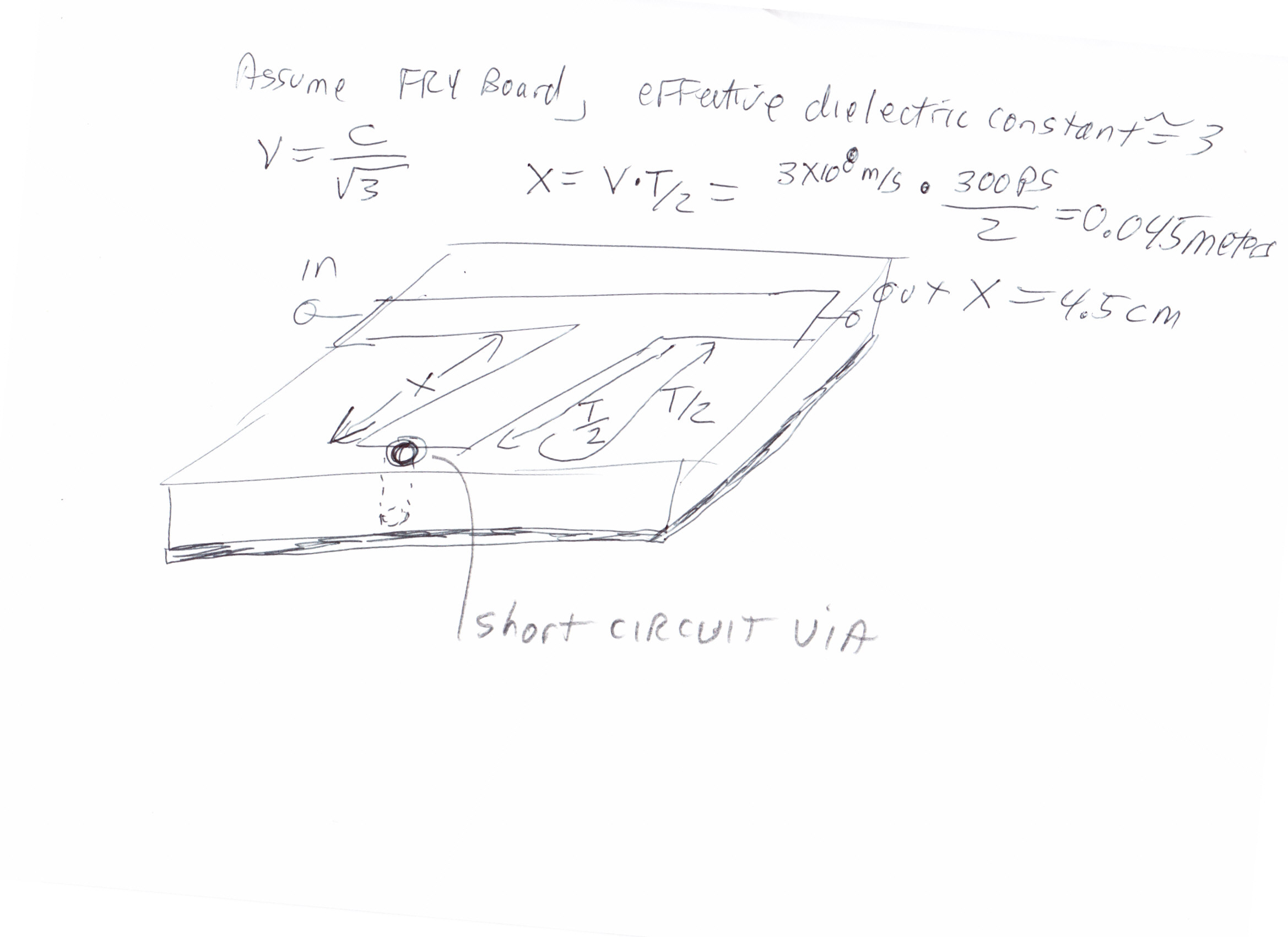
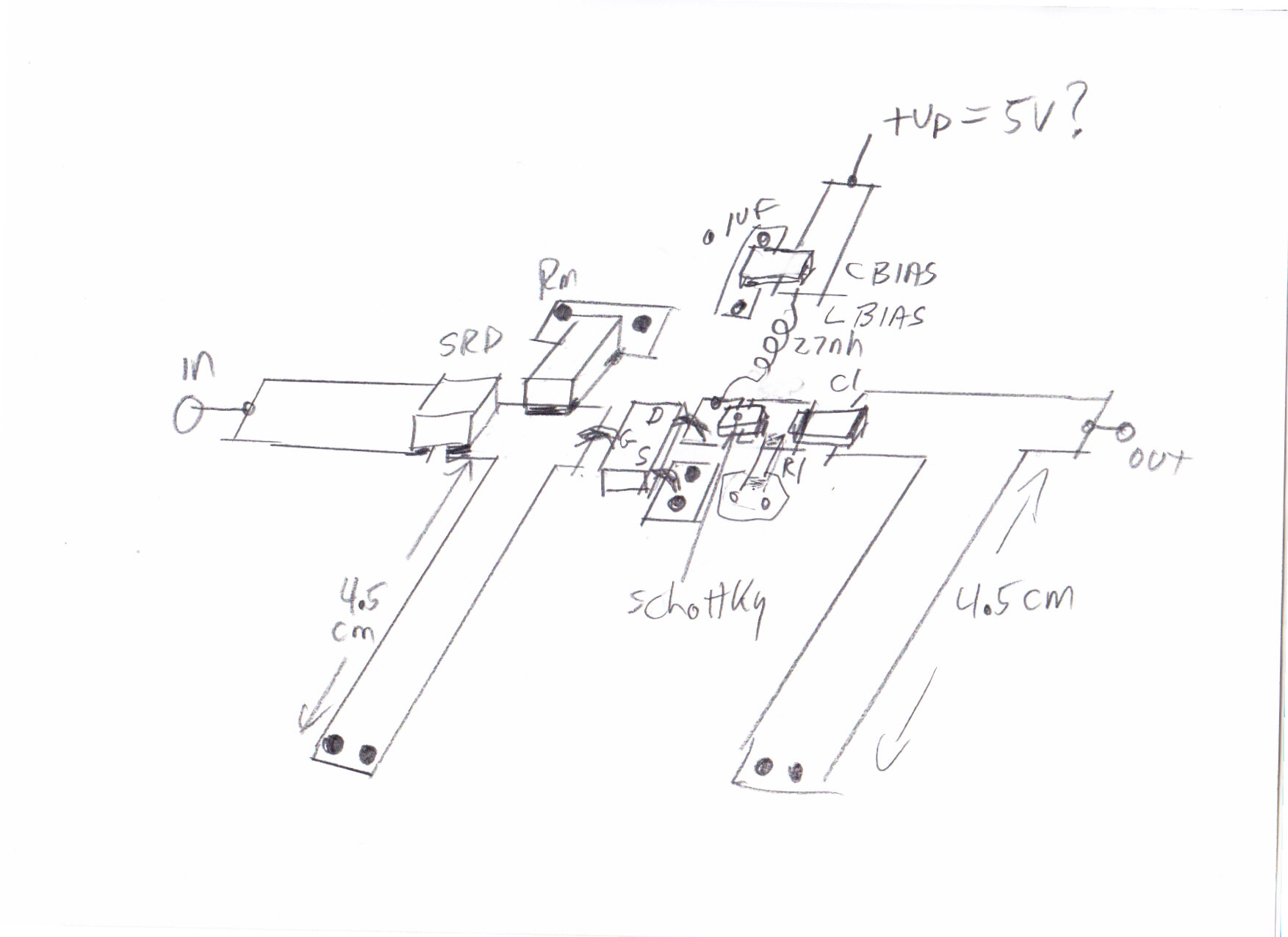
This is a 300pS pulse genearation using SRD.
Here Im not clear in SHORT CIRCUIT STUBS.
Please help me how can I Implement this Stubs in PCB?

Also the output of the generated pulse Impedence is 50 Ohm.
But I want to feed this to 25 Ohm load. How can i acheive by IMPEDANCE matching network.Whether it is possible to get any impdence matching readymade componens?
 

Voltage pulse comes up to a juncion. Voltage wave continues on past the junction, while another voltage wave travels up the stup. Some time later that voltage wave on stub hits a short circuit. Transmission line theory says that for 0 V across the short circuit, to cancel the forward traveling voltage wave, a reverse wave of equal amplitude but opposit sign travels back. Traveling from the junction to the short take T/2 seconds, and traveling back from the short circuit to the junction takes another T/2 seconds. When the return wave hits the junction, the total pulse ends. So, T=300 ps.


The confusing part of that paper is, like a scientist, they left off important components from the schematic, like biasing components! I added an inductor and capacitor on the drain to inject Vdc. You might have to add similar parts on the gate to control the gate bias voltage from something other than 0Vdc.

---------- Post added at 01:54 ---------- Previous post was at 01:46 ----------

 
Last edited:

    V

    Points: 2
    Helpful Answer Positive Rating
Replay to biff44
Date: 26th July 2011
Dear biff44

I would like to express my extreme thanks to your effort you have taken.
From the Replay impulse generation STUB design is okay.
But still some ambiguities and Stub length calculation mistakes.


As per the Equation V is related Effective dielectric constant
V=C/√3…………………. (1)
X=V*T/2…………………. (2)
From Eq (1)
X= (C*T) / 2*√3………. (3)
Here C=3*10^8 m/s; T=300ps;

So X= (3*10^8 m/s)*(300ps)/ 2*√3;
X=3.12Cm;
Let me ask my doubts.
1. More than 1 GHz FR4 is better or not?
Since here we are planning for 300ps. In terms of the frequency of operation which lies more than 3GHz.
Here you are designed the PCB in FR4 material. Instead of FR4 if we are using ROGER3003 (Effective dielectric constant is 3-6) or NELCO (Effective dielectric constant is 3.7) material results betterment in reduction in stub length.
2. SRD Biasing & input TTL signal
As per the Reference document SRD is neither foreword nor reverse in normal condition but on the arrival of input TTL signal SRD goes to reverse bias which results a negative impulse.
According to the analysis of Hamilton
(J.L. Moll, S.A. Hamilton, Physical modeling of the step recovery diode for pulse and harmonic generation circuits", Proc. Of IEEE, Vol.57, No.7, pp.1254 {1255, 1969.)
T1 = TR *ln*(1 + IF / IR) ------------------- (1)
When IF<<IR
T1 = TR (1 + IF / IR) ------------------------- (2)
Where
T1 is the reverse recovery time
TR is carrier lifetime
IF-Foreword current
IR- Reverse current.
Eq. (1) shows that T1 is proportional to TR, which also has relation to the ratio of IF and IR

So can I use the SRD in foreword bias (Adjustable Biasing voltage< TTL voltage)

Refer fig no: 1
**broken link removed**
FIG: 1

The –VEE required or not?


3. IMPEDANCE controlled PCB?
Whether I need to keep the PCB traces are 50 Ohms by impedance controlled PCB design?

4. MMIC AMPLIFIER & IMPEDANCE MATCHING

Can I amplify the generated 300ps signal in terms of V & I (2V, 4500mA) with the help of MMIC amplifier and interface this signal with input impedance 25 Ohms?

Selected MMIC amplifiers CHIPs are WIMAX AMPLIFIER chips from RFMD
Bias supply: 5V
Current – Supply: 800mA

So the output of the MMIC having Source impedance 50 Ohm
Let we assume
Vout (max) = 5V
I out (max) = 800mA @50Ohms

I need to interface this to 25 Ohms impedance with 2V, 400mA Can you suggest a practical circuit with design components?

Here I am attaching word doument too
 

word document attachement
 

Attachments

  • Discussion.rar
    312.8 KB · Views: 76

sorry, forgot the √3 divisor in the velocity! BTW, that is just a guess, you need to design the impedance of that stub (microstrip), and the actual εr varies with line width. You WILL get better results with a Rogers type board--lower loss.

I did not read the full paper, just looked at the schematic. The SRD is a device that conducts current in the forward direction forever, but conducts current in the reverse direction just momentarily (until the electrons are swept out of its I region). They are probably countin on this effect to let the rising edge of the pulse to go through, but make the falling edge of the pulse happen sooner than the input would suggest. I am not sure exactly how well this circuit would work...

As far as the mmic amplifier following it, to maintain the pulse shape, you will want a very broadband amplifier, as a 1st step. The 5th harmonic of 1/300 ps period is 10 GHz, not 3 ghz.
 

Replay to biff44

"As far as the mmic amplifier following it, to maintain the pulse shape, you will want a very broadband amplifier, as a 1st step. The 5th harmonic of 1/300 ps period is 10 GHz, not 3 ghz"

Let me Ask one question
The output formed is a monopulse with 300ps width.The PRF ranges from 1ms to 1microsecond.So may I want to keep the above
chara MMIC ?
 

1. More than 1 GHz FR4 is better or not?
You should use RO3003, but RO4350B is better because it's more robust than RO3003.
 

Status
Not open for further replies.

Similar threads

Part and Inventory Search

Welcome to EDABoard.com

Sponsor

Back
Top