Welcome to our site! EDAboard.com is an international Electronics Discussion Forum focused on EDA software, circuits, schematics, books, theory, papers, asic, pld, 8051, DSP, Network, RF, Analog Design, PCB, Service Manuals... and a whole lot more! To participate you need to register. Registration is free. Click here to register now.
The S-parameter analysis (S21=18dB, S11=-23dB) of the power amplifier is perfectly matched but output power is extremely low. How can I improve the output power?
Output Power Level of an Amplifier depends on few factors more not only matching.
-Operating Point and Biasing Current
-Available Power from the Amplifier by Load Pull Measurements ( Optimum Load for max. Output Power )
-Input Matching that ensures the available power from the source is delivered to Amplifier
20dBm is not a high Power Level. Even medium power transistors ( FET or BJT ) may provide this level.
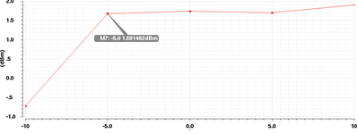
As I understand from your curve, the amplifier is wrong biased because the Transfer function is not regular. Check you biasing conditions
Hi
Make sure you carefully follow the design procedure:
1) Refer to transistor's datasheet and invoke the source and load impedances to be matched with transistor in the frequency of interest (Zs, ZL)
2)perform source/load pull simulation in ADS to find the best Zs and ZL to meet the delivered power and power added efficiency (PAE) requirements of your design.
2) Design the input and output matching networks to match 50 ohm line to Zs and ZL
3)perform load pull simulation again in presence of matching networks again and modify the designed matching networks to get the best result.
This site uses cookies to help personalise content, tailor your experience and to keep you logged in if you register.
By continuing to use this site, you are consenting to our use of cookies.