Continue to Site

Welcome to EDAboard.com

Welcome to our site! EDAboard.com is an international Electronics Discussion Forum focused on EDA software, circuits, schematics, books, theory, papers, asic, pld, 8051, DSP, Network, RF, Analog Design, PCB, Service Manuals... and a whole lot more! To participate you need to register. Registration is free. Click here to register now.

RF Power Amplifier-- Beginners Questions..Getting input power from datasheet..

Status
Not open for further replies.

themaccabee

Full Member level 4
Joined
Apr 1, 2007
Messages
201
Helped
6
Reputation
12
Reaction score
6
Trophy points
1,298
Activity points
3,003
Hi,

Im totally new to RF circuits, i need to find the maximum input power that can be given to the Power Amplifier MWE6IC9100NBR1(datasheet attached)
I went through the datasheet ,, and it gives a equivalent Circuit diagram like below
53_1293693054.jpg

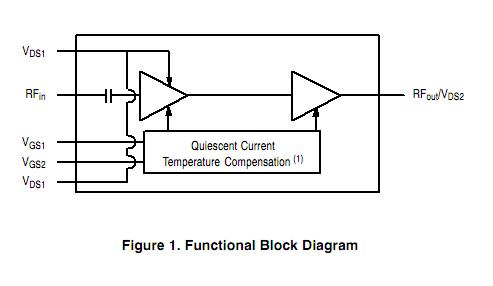
But the datasheet doesnt mention abt any absolute maximum rating for RFin signal..
Im confused ,, maybe isnt that way should i look for that information??

The data sheet do say about output power,efficiency etc,,should the maximum input power need to be obtained in that way??
Regards
Steve
 

Attachments

  • MWE6IC9100N.pdf
    845.8 KB · Views: 113

I think the problem is now solved...
The maximum output power is mentioned as P1dBm=100W=50dBm@960MHz subtracting the gain =33 gives 17dBm maximum input power level.
Hope it is that way
Regards
Steve.
 

Re: RF Power Amplifier-- Beginners Questions..Getting input power from datasheet

You closed your thread before we could answer. You seem to have overlooked the line in the data sheet that says:
"TABLE I: Maximum Ratings, Gate-Source voltage: -.5 to +6 V"

So, if your gate to source voltage, at any instant in time, exceeds that voltage range, you will degrade or possibly blow out that device.
 

Hi biff44,
You seem to have overlooked the line in the data sheet that says:
"TABLE I: Maximum Ratings, Gate-Source voltage: -.5 to +6 V"
But..hmm.. Gate to source voltage is for the VGS1&2 signals right??The datasheet is saying that it is used for Quiescent Current Temperature compensation..I hope it is for maitaining some dc biasing current isnt it so?? Correct me if im wrong..
So the initial question was about the RF signal IN not about the VGS1&2 thats why i assumed the input power giving a safe margin so that the output never goes to 1dB compression value..

Please post your view on this matter..
Regards
Steve
 
Last edited:

Status
Not open for further replies.

Part and Inventory Search

Welcome to EDABoard.com

Sponsor

Back
Top