Continue to Site

Welcome to EDAboard.com

Welcome to our site! EDAboard.com is an international Electronics Discussion Forum focused on EDA software, circuits, schematics, books, theory, papers, asic, pld, 8051, DSP, Network, RF, Analog Design, PCB, Service Manuals... and a whole lot more! To participate you need to register. Registration is free. Click here to register now.

RF Harvesting Circuit

Status
Not open for further replies.

Burwhite

Newbie
Joined
Jun 16, 2020
Messages
4
Helped
0
Reputation
0
Reaction score
0
Trophy points
1
Activity points
30
Dear Members,

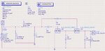
I have designed a RF Harvesting circuit at 5200 MHz. I used Dickson Voltage Mutiplexer (2nd grade) and L type impedance matching network. I am having some trouble about the output voltage. It is about 1.733*10-4.

1. Is my circuit design appropriate/correct?

2. Why the output voltage is too low?

3. What can I do for getting the highest voltage?


1592307743995.png


Thanks.
 
Last edited:

Your posted schematic is not clear.
I found in a paper a similar circuit as yours but working on 915MHz. Simulate this one (with the components provided in the picture), and if is working, just change with the values you have for 5.2GHz.
 

Attachments

  • Dickson.jpg
    Dickson.jpg
    98.2 KB · Views: 169

The circuit is that reported in the paper "Analysis of Dickson Voltage Multiplier for RF Energy Harvesting" and it works. You have a much higher frequency and of course a different matching.
The attached image is poorly defined so I can't read the value of the matching LC, the input power, the load resistance and the diodes you used.
It should work at least in simulation. In case of real implementation at this frequency many more parameters have to be taken into account.
 

I posted a clear picture. The diodes are HSMS2852.
 

The input power of -19dBm (corresponding to 25mV @50ohm) is definitely too low.
 

In most of the cases, -15dBm (30uW) input power for harvesting is good only to write a paper, but to get real efficiency you have to hug the antenna of a cellular base station :)
 
  • Like
Reactions: vivekroy

    d123

    Points: 2
    Helpful Answer Positive Rating
There are two things that can the increase the output voltage.

1. Match the input impedance. After you have done this, the return loss (at low power) will be <= -10 dB as in AN 1156 fig. 8 and the output voltage vs freq graph will show a peak at your design frequency as in **broken link removed** fig. 12.

2. Increase the output load from the existing 50 kOhm to the MOhm range. The quadrupler has a high output impedance and loading it will decrease output voltage.

All the above is for simulating with ideal components only. If you want to simulate a real circuit at 5.5 GHz, your circuit model will need to account for component parasitics. Additionally, the SOT-323 packaged HSMS-285c will have less parasitic than the SOT-23 HSMS-2852. You will likely need to fine-tune every board as the HSMS-285x family has poor consistency above 1 GHz.
 

In most of the cases, -15dBm (30uW) input power for harvesting is good only to write a paper, but to get real efficiency you have to hug the antenna of a cellular base station :)
I always wondered if we can do better by flying a drone over the wireless sensor node equipped with the harvesting tag.
 

Status
Not open for further replies.

Part and Inventory Search

Welcome to EDABoard.com

Sponsor

Back
Top