Continue to Site

Welcome to EDAboard.com

Welcome to our site! EDAboard.com is an international Electronics Discussion Forum focused on EDA software, circuits, schematics, books, theory, papers, asic, pld, 8051, DSP, Network, RF, Analog Design, PCB, Service Manuals... and a whole lot more! To participate you need to register. Registration is free. Click here to register now.

RF CMOS Bandpass Filter using active inductor

Status
Not open for further replies.

diyanasri

Newbie level 4
Joined
Nov 14, 2008
Messages
6
Helped
1
Reputation
2
Reaction score
1
Trophy points
1,283
Activity points
1,335
Hello everyone,

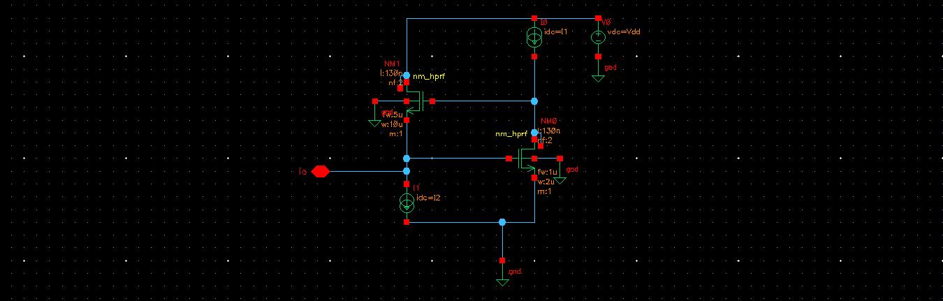
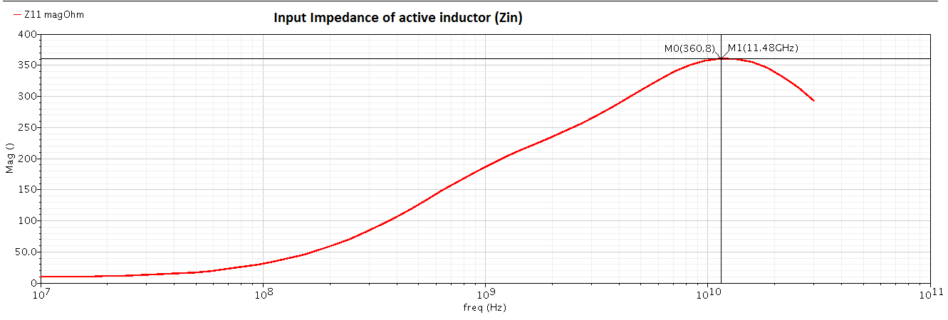
I'm trying to design a CMOS bandpass filter (BPF) using active inductor. Basically I think I got the active inductor part working.

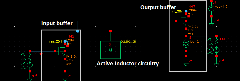
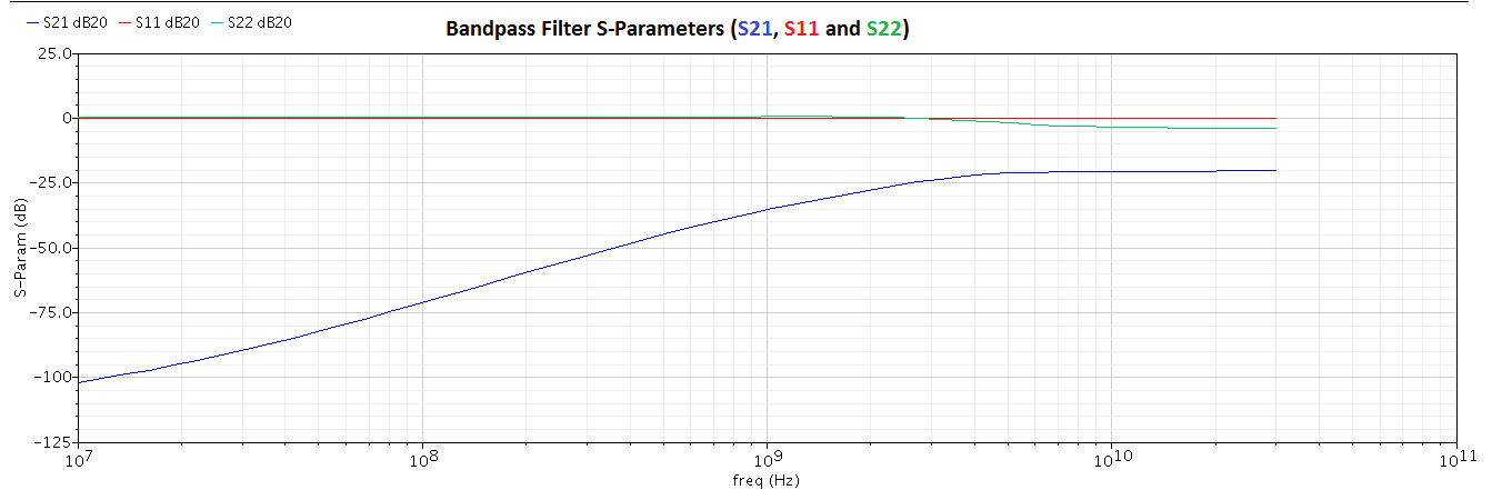
The BPF is based on topology mentioned in Fei Yuan book where input signal goes through input buffer - active inductor - output buffer. However when I try to implement the active inductor circuit into a BPF and do S parameter analysis, it starts giving problems. I am getting S21 (dB) plot that looks something like a very lossy high pass filter.

I suspect it's the buffer circuits that's giving problems. Is there something I am missing?:?:

Please help me out guys and girls.
 

Hi,

Sorry for the incomplete question and keeping you waiting. Was swamped with meetings and talks.
Anyway, here are my circuits and their responses. I am using Cadence virtuoso and Analog Design Environment for simulations.

- The first one is the basic active inductor circuit and it's input impedance Zin.


- The ssecond one is I try to implement the active inductor into a bandpass circuitry according to notes mentioning having input and output buffer connected to the active inductor. However when I ran S-Parameter simulation, I'm getting a high pass filter instead of a bandpass filter and the insertion loss is very high.


My question is, is the bandpass circuit correct? Where did I go wrong.
I would very much appreciate your input.
 
I also studying this circuit, it's not work as paper described.
@diyanasri : have you still working on LNA using active inductor?
 
diyanasri,
For my opinion, the inductor impedance looks not to bad.
Try a linear scaling on the frequency axis and you will see a curve that perhaps can satisfy you.
But be aware, that you haven't build an ideal inductor. Thus, there are series and parallel losses which - among other effects - are responsible for the bad high frequency behaviour.

As far as the filter is concerned, I see two buffers (is the 1st one really necessary?) and the inductor.
Where is the capacitor?
 

LvW:
Do you mean having a capacitor in parallel to the Inductor?
My aim is to use the intrinsic capacitances of the Mosfet Cgs to interact with the simulated inductance. At some point higher up the frequency, the circuit L and Cgs will resonate.
You are right, the 1st buffer is not necessary. But i fail to get any good S21 response.
I'm still looking through published papers to understand how the buffers work. Not much success though.

Bicave:
No, i'm not working on LNA, but on bandpass filter. You can ask me about simulation of the active inductor.
 

My aim is to use the intrinsic capacitances of the Mosfet Cgs to interact with the simulated inductance. At some point higher up the frequency, the circuit L and Cgs will resonate.

"At some point"......OK, but don't you intend to design (that means: to choose) the resonant frequency? Don't forget, your active inductor works as an inductor in a limited frequency band only.
 

Status
Not open for further replies.

Similar threads

Part and Inventory Search

Welcome to EDABoard.com

Sponsor

Back
Top