Continue to Site

Welcome to EDAboard.com

Welcome to our site! EDAboard.com is an international Electronics Discussion Forum focused on EDA software, circuits, schematics, books, theory, papers, asic, pld, 8051, DSP, Network, RF, Analog Design, PCB, Service Manuals... and a whole lot more! To participate you need to register. Registration is free. Click here to register now.

Resistive Feedback Bode Plot Problems

Status
Not open for further replies.

Arielle

Newbie level 6
Joined
Aug 8, 2013
Messages
13
Helped
0
Reputation
0
Reaction score
0
Trophy points
1
Activity points
110
Hi guys,
I have a very fundamental problem: First, is it possible to use resistive feedback on a circuit as shown in the picture? When I tried to simulate it, the bode plot had a very odd form and the DC gain I calculated by -Rf/Rin could not be seen in the simulation results... Help pls.
300px-Op-Amp_Inverting_Amplifier.svg.pngota.png
Arielle
 

Those are not identical circuits. The circuit on the right is a simple differential to single-ended amplifier which has a DC offset between the input and output. You can not use straight resistive feedback with that. You need a level shifter output stage and frequency compensation to operate as an op amp, similar to that shown in the left picture.
 
Your OTA is not bufffered, so by adding resistive feedback You decrease an open loop gain of amplifier from gm2(rds2||rds4) down to gm2(rds2||rds4||Rf). So if Rf<<(rds2||rds4) a small signal gain of amplifier goes below 0dB. In addition if You have unipolar power supply (e.g. gnd and +vdd only) You should put your small signal ground on some level, e.g. vdd/2 to provide correct dc operating point. Of course You should remember about output current limitation - your feedback current shouldn't be higher than current flowing in amplifier branches.
 
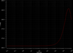
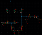
Hey, thank you two! I tried to do as you said (see screenshot) and I think that my gain can be set by Rfb/Rin now. However, my phase is... not what I expected and if I apply larger AC signals than 1mV at the input, my output common mode goes up. I made pictures and hope, you can tell me what I did wrong... ;__;
Transient_out.PNGVGA_Phase.PNGVGA_resistives_Feedback.PNG
 

Now You added second amplifying stage so you have to add compensation RC network to ensure stability (look for miller opamp). I mean buffered stage → simple source follower to provide low output impedance to drive resistive feedback.
 
Hey, thank you two! I tried to do as you said (see screenshot) and I think that my gain can be set by Rfb/Rin now. However, my phase is... not what I expected and if I apply larger AC signals than 1mV at the input, my output common mode goes up. I made pictures and hope, you can tell me what I did wrong... ;__;

Arielle, I really don`t know what you are asking.
I see a differential amplifier (with a high resistive output: OTA) and a second stage.
Please note that one amplifier input node is OPEN !
You speak about feedback, but where is your feedback path?
What is your goal? Amplification with resistive negative feedback ?
Why do you inject a signal into the OUTPUT?
 

Hi guys, just wanted to say that it's finally working & thank you very much for your help. After I inserted a buffer (instead of a second stage hahaha), it worked out =)
@LvW: sry, my screenshot was bad because it didn't show that I had actually a signal at the second input, so it's not open
 

Hi guys, just wanted to say that it's finally working & thank you very much for your help. After I inserted a buffer (instead of a second stage hahaha), it worked out =)
@LvW: sry, my screenshot was bad because it didn't show that I had actually a signal at the second input, so it's not open

OK fine. So it is "working". And you are sure that the results are correct?
 

Status
Not open for further replies.

Similar threads

Part and Inventory Search

Welcome to EDABoard.com

Sponsor

Back
Top