Continue to Site

Welcome to EDAboard.com

Welcome to our site! EDAboard.com is an international Electronics Discussion Forum focused on EDA software, circuits, schematics, books, theory, papers, asic, pld, 8051, DSP, Network, RF, Analog Design, PCB, Service Manuals... and a whole lot more! To participate you need to register. Registration is free. Click here to register now.

resistance current limit

Status
Not open for further replies.

yassin.kraouch

Advanced Member level 2
Joined
Jul 5, 2009
Messages
631
Helped
40
Reputation
80
Reaction score
40
Trophy points
1,308
Activity points
5,094
Hi All,

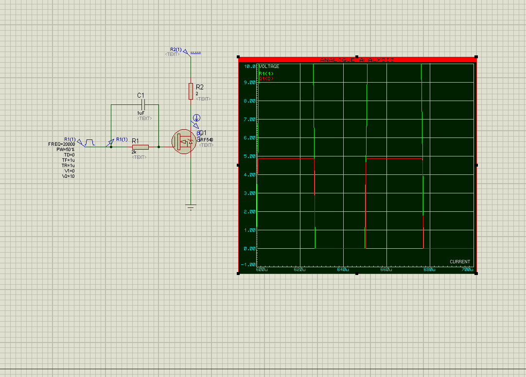
how can i calculate the resistor value in order to limite the current consumption, from a circuit : i have a gate of a MOSFET transistor that i would like to connect it to a microcontroller, but the microcontroller can only deliver 25 mA maximum value,
 

Attachments

  • Sans titre.png
    Sans titre.png
    83.5 KB · Views: 83

mosfet are not based on current, not like BJT.. they use the voltage applied on gate as a reference.
the most commun is put a high value resistence in gate.

search for how mosfet works on web, may answer your doubts.
 

mosfet are not based on current, not like BJT.. they use the voltage applied on gate as a reference.
the most commun is put a high value resistence in gate.

search for how mosfet works on web, may answer your doubts.

Can you explain the existence of high current mosfet drivers, why do they exist if you can drive the mosfet with a high value resistance?
For example TC4427 **broken link removed** , can sink/source 1.5A and I can give you examples of drivers with higher currents.

I would suggest you read https://www.edaboard.com/threads/196377/
If you are still in doubt you can read something like **broken link removed**

Alex
 

yes i agree with alexan_e therocially there no current but in practice there is a current in order to charge the gate capacité, the problem is how to limit the current? can anyone help us to resolve this problem ?
 

With a constant voltage it is very easy to limit the current, the problem is that we have an mcu output with a high internal resistance that drops the voltage to 0v at about 25mA.
The mcu is MSP430 and the output voltage graph is like this
MSP430_output_current.jpg
The current will obviously be limited by the internal resistance but in this case there will be periods where the voltage will be very low, I don't know if there is a way to limit the current to 7mA so that the min output voltage stays at 2.5V.
This resistor is going to drive a mosfet, you can see the discussion https://www.edaboard.com/threads/213813/

@Iuri
An image is usually better than words, you can easily see the difference in the output current with the same mosfet driven using 5mA and 1A
The red line is input voltage and the blue is output current, the input is 10v pulses 50% at 20KHz.
Apart from the obvious distortion in the wave of the output you will also have overheat problems with the upper mosfet.
mosfet_drive_compare.jpg

Alex
 
Last edited:

I never worked with MOSFETs in practice, just in theory, so for me the gate current was always near to 0A... that thread you linked before opened my eyes, now I see the difference, thanks alex. But I can not see why this will overheat.

sorry yassin for the off-topic.
 

the steps that the mosfet goes through while conducting are shown inthe next image (from page 17 of https://www.fairchildsemi.com/an/AN/AN-9010.pdf ),
Mosfer_gate_charge.jpg

The output current is shown with green, the voltage drop across the mosfet is shown in blue.
The X axis shows the different stages while the mosfet capacitance gets charged
Between t1 and t2 the output current goes from 0 to the max , in that point you still have the max voltage drop across the source-drain and also the max current through the mosfet that means many watts as heat (V*I).
As the charge stages go on you see that the voltage drop across the mosfet lowers at the t2 to t3 stage where it goes almost to 0
You want to provide high current to the gate to go through that stages as soon as possible because the part from t0 to t3 is a high power consumption stage.
You can either do that id a few nano seconds or it can take many us and even ms.
Also note that the mosfet goes through this stages when it turns off too and consider that it goes through them 40000 times per second with a PWM of 20kHz (20000 times on and 20000 times off)

Alex
 
Last edited:

The output of a mcu I/O is a mosfet. The size of the device determines its channel resistance and therefore its driving capability.

In driving a MOSFET there are current spikes during the transitions where the gate is being charged and discharged. The average current will be CVF where C is the equivalent input capacitance of the MOSFET, V is the gate driving voltage, and F is the switching frequency.

Normally all you have to do is make sure you have a sufficient decoupling cap on the mcp GPIO supply line. Don't worry about the 25 mA max drive unless it is insufficient to get the risetime you need for the mosfet gate drive, or you are switching so fast that the CVF is more then about 15% the 25 mA drive limit. The decoupling cap will supply the transition surge current. You want to use a ceramic cap with low ESR. A 0.1 uF normally does the job.

Input capacitance of MOSFET is more then the gate capacitance due to Miller effect. MOSFET manf. have created a spec called gate charge, spec'd in coloumbs. Required peak driving current to achieve a desired slew rate is gate charge/slew time.

Usually the bigger issue is the I/O driving voltage. If you only have a 5v I/O you may not have a high enough gate voltage to get a low Rds-ON resistance for the MOSFET. Most power MOSFET's are specified for 10v to 15v gate drive. Any MOSFET's Rds-ON is a function of gate drive voltage.

'Logic' drive level MOSFET's are mostly just large devices to get a low Rds-ON for a lower gate voltage. The larger the device the more the gate input capacitance.
 
Last edited:


the steps that the mosfet goes through while conducting are shown inthe next image (from page 17 of https://www.fairchildsemi.com/an/AN/AN-9010.pdf ),
View attachment 56675

The output current is shown with green, the voltage drop across the mosfet is shown in blue.
The X axis shows the different stages while the mosfet capacitance gets charged
Between t1 and t2 the output current goes from 0 to the max , in that point you still have the max voltage drop across the source-drain and also the max current through the mosfet that means many watts as heat (V*I).
As the charge stages go on you see that the voltage drop across the mosfet lowers at the t2 to t3 stage where it goes almost to 0
You want to provide high current to the gate to go through that stages as soon as possible because the part from t0 to t3 is a high power consumption stage.
You can either do that id a few nano seconds or it can take many us and even ms.
Also note that the mosfet goes through this stages when it turns off too and consider that it goes through them 40000 times per second with a PWM of 20kHz (20000 times on and 20000 times off)

Alex

Now I see, thx Alex.
 

You may also find this useful, it is the power consumption on the mosfets in the circuits of my previous post (voltage drop across drain-source multiplied with the drain current).
It shown the power consumption (left axis watts) vs time (y axis) for one period , red=1A gate current and blue=5mA gate current

mosfet_switching.gif

Alex
 

what do you think about adding a cap in parallel with the resistor ?
 

You are dealing with a 20KHz signal, the capacitor is bypassing the resistor and the current goes through it.
The impedance of the capacitor is 1/2πfc , in your case 1/(2*3.14*0.000001*20000)=7.95 ohm.
Instead of bypassing you might as well use a lower resistance.
The problem in your case is that the source has not a low impedance like in the schematic, if you want to simulate something close to the behavior of your source add a 133 ohm resistor to your source and then use any gate circuit you like.
If you use a probe in the gate you can see what is the current that goes to the gate.

Alex
 

what do you think about adding a cap in parallel with the resistor ?
I think, you can omit two components, place a short instead and get basically the same effect: The current will be only limited by the processor output driver, and surely exceed the specified maximum values.

RCinFLA mentioned, that short current spikes exceeding the maximum current must not necessarily be a problem or even damage the processor. I tend to agree, but I would prefer either current limiting resistors or strong external drivers, if fast MOSFET switching is needed.
 

FvM , can he get more current that the max shown in the output graph of the datasheet or this graph applies in any case?
For example can he get 100mA?
Will the voltage drop shown in the graph be applied is short pulses (while charging the gate), if it is then with 25mA the output will be 0, how can he get more current?
Do you think he can drive the mosfet with a PWM of 20KHz using that mcu?

MSP430_output_current.jpg

Alex
 

yes i agree with you, but the speed up capacitor is included so the resistor do not slow the gate charging process

---------- Post added at 10:41 ---------- Previous post was at 10:27 ----------

alex : how did you know the internal resistance of the mcu ?
 

FvM , can he get more current that the max shown in the output graph of the datasheet or this graph applies in any case?
Not when driving a MOSFET gate. But the characteristic doesn't apply to all processor ports. There are many, that are able to source or sink current above maximum ratings. If not, the current limiting resistor discussion would be void.

You should remember a similar thread related to Freescale MC9S08AC60CFGE. The processor has a programmable drive strength, with low drive strength, maximum ratings are kept even for high capacitance loads, but with high setting, they can be exceeded.
https://www.edaboard.com/threads/199039/
 

if you take a couple of points from the mcu output curve you can calculate a resistor that has a voltage drop similar to the graph, it will not be exact because it is not a line but a curve.

Alex
 

the other idea is to connect 3 or 4 pin from the microcontroller together to deliver more current ( for example 4 pins can deliver 4*25 ma), is this a good idea ?
 

Not when driving a MOSFET gate. But the characteristic doesn't apply to all processor ports. There are many, that are able to source or sink current above maximum ratings. If not, the current limiting resistor discussion would be void.

Sorry for my questions but I'm trying to understand if the output is different from what I think it is.
The mcu is https://focus.ti.com/lit/ds/symlink/msp430f133.pdf
The graph shows a voltage drop as the current gets higher , it is like in internal resistance which "limits" the current to 25mA since the output at that current is 0v, is it possible to get more current when the output is already in 0v?
Is there a case that you can get a current in the output that doesn't have that voltage drop?
Do you mean that if the current surge is very short you don't get that voltage drop?
If so how can I calculate this time, is it shown as an output capacitance which can discharge without having a voltage drop?

Thank you
Alex
 

Status
Not open for further replies.

Part and Inventory Search

Welcome to EDABoard.com

Sponsor

Back
Top