Continue to Site

Welcome to EDAboard.com

Welcome to our site! EDAboard.com is an international Electronics Discussion Forum focused on EDA software, circuits, schematics, books, theory, papers, asic, pld, 8051, DSP, Network, RF, Analog Design, PCB, Service Manuals... and a whole lot more! To participate you need to register. Registration is free. Click here to register now.

replica-feedback biasing for differential delay element

Status
Not open for further replies.

Fractional-N

Full Member level 1
Joined
Oct 15, 2007
Messages
97
Helped
2
Reputation
4
Reaction score
2
Trophy points
1,288
Activity points
2,071
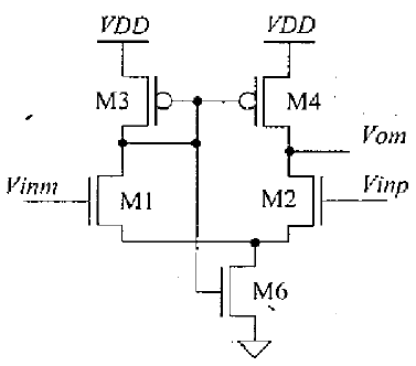
the circuit below is a replica-feedback bias circuit for a differential delay element.


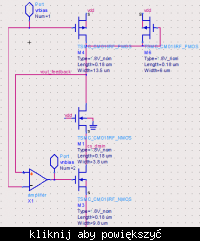
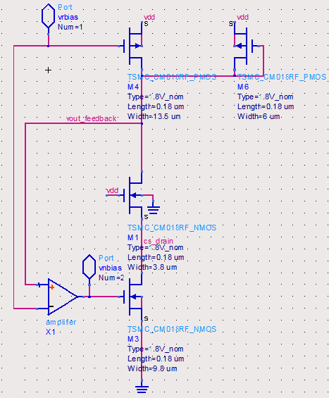
when I simulate the delay chain with this bias circuit, there is a large sensitivity over supply voltage (Vdd); while there shouldn't be. I mean the circuit is not supply insensitive. can anyone help me? does this kind of biasing really work?

thanks
 

I think your circuit is misconnected, the FET attached to the
vout_feedback should have gate to the other PFET and drain
to the feedback node.
 

    Fractional-N

    Points: 2
    Helpful Answer Positive Rating
dick_freebird said:
I think your circuit is misconnected, the FET attached to the
vout_feedback should have gate to the other PFET and drain
to the feedback node.
i don't know what you mean. can you explain more clearly?

Added after 5 hours 36 minutes:

here is some more information about my simulations.
I simulated two differential delay chains.
first one WITHOUT replica-feedback bias circuit, when I change vdd from 1.75 to 1.85, delay between stages change from 50p to 61p (10p change in delay).
second one WITH replica-feedback bias circuit, when I change vdd from 1.75 to 1.85, delay between stages change from 47p to 68p (20p change in delay).
obviously the sensitivity to supply voltage is more when I use replica feedback biasing. but replica-bias should make the circuit insensitive to supply. can anyone help
 

There is unlikely that your transistor actually do have four pins.
 

    Fractional-N

    Points: 2
    Helpful Answer Positive Rating
That is not strange. It simply using a 4-terminal NMOS-symbol for design in a process where the NMOS does not have a "free" body terminal. Not everyone could affort a supported designkit and a cadence license.


The problem with replicate bias in ringosc is that it focus on supply independend current source generation. I did not analyse your circuit in detail. But this focus will overlook that the signal swing and switching is still impacted by the supply.

Then change the direction of the focus!

Use a uncontrolled ringosc and use directly the supply of this ringosc as control voltage. Use some cap, which could be MOS-cap as supply for ripply filtering. Then drive the supply with a PMOS-current source. The PMOS-gate is control voltage of the ringosc. The supply impact is now coming from changing current source value but this could be much better controlled than a replicated ringosc circuit where you have many other impacts. The lower level clock could be level translated. True there is also a supply effect but this is only through drain/gate-cap which could be reduced by cascode withhin the level shifter.
 

    Fractional-N

    Points: 2
    Helpful Answer Positive Rating
Is it a symmetrical load delay stage?

a few thoughts:
1, How about the PSRR of your amplifier?
2, the upper two PMOSs, the size is not identical, are you intend to do that?

BTW what's the transistor ratio between this replica and the delay stages
 

    Fractional-N

    Points: 2
    Helpful Answer Positive Rating
strennor said:
Is it a symmetrical load delay stage?
Yes,
actually i wanted to use maneatis delay stage. If I have understood correctly the symetrical load is necessary to lower dynamic jitter; and replica feedback biasing lower static jitter. My circuit (without symetric load) shows a great amount of static jitter, and this is my problem. i designed a delay cell with identical PMOS transistors both the result was the same. The amplifiers duty is to equate voltages at two input nodes, and it does it perfectly. i haven't considered its PSRR. does it have a large effect on jitter?

it seems to me that maneatis method of designing a supply independent delay cell, does not really work. because although it stabilizes min voltage value, the max voltage value(hence the swing) is still dependent on supply voltage, and therefore, amout of delay changes with supply voltage variation.

This is the exact replica. the ratio is one.
 

1, i think the replica amplifier should be fast enough, the high frequency psrr should be good enough. is your amplifier an ideal one?

2, i read a document. the transistor ratio, between replica and delay cell, is 1:1 for loads, but 0.5:1 for the tail current source. What's your idea?


3, i think, any delay stage has supply introduced jitter.

the symmetrical load is good because it is symmetrical. but it isnot unaffected by supply noise. if very good psrr is required, why not use a regulator for your positive supply?
 

    Fractional-N

    Points: 2
    Helpful Answer Positive Rating
1- it is a very simple amplifier
96_1271780062.png


2- because the delay cell is in one of switching states at any point of time, tail current flows in one of branches, so tail current source ratio is also 1:1.
3- so what is the benefit of maneatis load and biasing method?
 

1, How about the amplifier offset? How about the amplifier PSRR? I see the amplifier tail current depends on supply voltage. Have you tried use an ideal amp in the replica? or an amp with very good psrr? Could the jitter be better?

3, there are many types of delay stages, but it has very large tuning range, ideally begins from DC. it is the biggest benefit i see
 

Yes,
actually i wanted to use maneatis delay stage. If I have understood correctly the symetrical load is necessary to lower dynamic jitter; and replica feedback biasing lower static jitter. My circuit (without symetric load) shows a great amount of static jitter, and this is my problem. i designed a delay cell with identical PMOS transistors both the result was the same. The amplifiers duty is to equate voltages at two input nodes, and it does it perfectly. i haven't considered its PSRR. does it have a large effect on jitter?

it seems to me that maneatis method of designing a supply independent delay cell, does not really work. because although it stabilizes min voltage value, the max voltage value(hence the swing) is still dependent on supply voltage, and therefore, amout of delay changes with supply voltage variation.

This is the exact replica. the ratio is one.

Hi, I hope it is not too late to reply. I have the same problem. But, I go back to the paper "Precise Delay Generation Using Coupled Oscillators" and found the control voltage is with respect to Vdd not ground which simply means the control voltage is fixed with the power supply varies. The replica biasing is just used to isolate the delay cell from negative supply or ground.
 

Status
Not open for further replies.

Similar threads

Part and Inventory Search

Welcome to EDABoard.com

Sponsor

Back
Top