Continue to Site

Welcome to EDAboard.com

Welcome to our site! EDAboard.com is an international Electronics Discussion Forum focused on EDA software, circuits, schematics, books, theory, papers, asic, pld, 8051, DSP, Network, RF, Analog Design, PCB, Service Manuals... and a whole lot more! To participate you need to register. Registration is free. Click here to register now.

removing gain and offset errors

Status
Not open for further replies.

yefj

Advanced Member level 4
Joined
Sep 12, 2019
Messages
1,189
Helped
1
Reputation
2
Reaction score
3
Trophy points
38
Activity points
7,172
Hello ,i have a 3 bit converter with idial LSB of 50mV ,The following table showing bellow the noon idial logical values.
I need to remove gain and offset errors from the codes bellow.
I read in the internet that one step to remove gain error is to calculate a new LSB by doing an avarage
AVG_LSB=(363-(-2))/(8-1)=52.14V
So if i calculate the table using this new LSB(NEW gain) i get table 2 shown bellow.
Did it remove the gain error?if so then Why its called removing gain error??
Thanks.

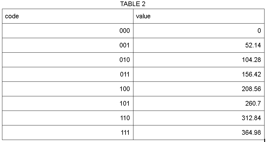
1600166788917.png

1600168023779.png
 

Hi,

maybe ADC, maybe DAC, maybe measured value, maybe calcutaed values, maybe one shot including noise, maybe not.....
We don´t know your circuit, nor your test circuit, nor your test conditions. Nor do we know what you want to achieve.

How can we help?

Klaus
 

Signal averaging, attached ap notes.


Regards, Dana.
 

Attachments

  • AtoD averaging.rar
    1.7 MB · Views: 86

The question is a theorectical one regarding the steps of the ADC its not analog issue
its logicall step voltage question
--- Updated ---

gain is the slope of the steps.
we have idial and not idial.
i dont understand the meaning of fixing gain error
--- Updated ---

In the article bellow they talk abut it but very unclear.
So in order to fix gain error i need to do avarage step and make the last code to be FULL scale
but if the step is larger then then LSB then its not possible.
what is the way we need to do to fix gain error?
1600188863868.png
).
 
Last edited:

Hi,

you say ADC.
there is not a fixed voltage for each step of an ADC, but there is a range.
like: for ideal case ADC
000 --> -200mV ... +25mV (lower voltage depends on absolute maximum input voltage range)
001 --> +25mV ... +75mV
010 --> +75mV ... +125mV
...
110 --> +275mV ... +325mV
111 --> +325mV ... +3300mV (upper voltage depends on absolute maximum input voltage range)

*************
AVG_LSB=(363-(-2))/(8-1)=52.14V
So if i calculate the table using this new LSB(NEW gain) i get table 2 shown bellow.
Did it remove the gain error?if so then Why its called removing gain error??
No. You dont remove any error. You just calaculate the average step size. That´s all.

And the output pf the ADC is still 3 bits 000 up to 111.
If you want to correct the digital value (with a microcontroller), then you need fixed point or floating point arithmetics with more than 3 bits of resolution.

Klaus
 

    yefj

    Points: 2
    Helpful Answer Positive Rating
Hello Klauss,Its not about microcontrollers :) i am studying general ADC theory definitions.
The theory says that in order to calculate DNL INL we need to remove gain and offset errors.
I got the consept the using the avarage step we recalculate all the degital levels 000 ..111
000->0*AVG_step
001->1*AVG_step
.
.
111->7*AVG_step
and for some reason the new step are considered to
be removed of gain and offset error.
If its true i cant see why it removed those errors.
how exactly do i remove them pen and paper looking at the ranges of each logical level?
i cant see the method.
Thanks.
 

Hi,

I really don´t understand.

an ADC has an analog input and a digital ouput.

To modify offset and gain you have two options. Either modify the analog side or you modify the digital side.
but you have to understand:

even on an ideal 3 bit ADC (your example)
if the input is 25.001V the output will be 001
if the input is 32.123V the output will be 001
if the input is 42.876V the output will be 001
if the input is 74.999V the output will still be 001

So from the output "001" you can´t detect whether the input voltage is 25.001V or 74.999V. So in my eyes it´s not useful to discuss about 0.140mV ( 52.14V - 52.00V) when the step size is 350 times the theoretical error.

with ADCs there´s always an uncertainty fo 1LSB (or +/- 0.5LSB) in your case 50mV.


Klaus
 

    yefj

    Points: 2
    Helpful Answer Positive Rating

Gain and offset error of a DAC is only an averaged quantity. Your table shows linearity errors which can't be compensated by adjusting gain and offset. What do you exactly want to achieve?

If you want to adjust gain and offset, it's a poor method to look only at the first and last value, as done in the post #1 gain correction. Instead you'll derive the line of best fit.
 

    yefj

    Points: 2
    Helpful Answer Positive Rating
How you remove gain and offset error depends
on how you built it. "Back in the day" when you
had decent natural device matching and good
device stability, you'd build in one-time trim
elements.

In CMOS with poor and time-variable offsets
you'd probably prefer an auto-zero for any
amplifier or comparator, and switch-based
resistor / current-source network corrections.

Wide ADCs sometimes have elaborate table
based correction applied after the A-D core
yields a number; cal-map, like.

Errors often come from asymmetries in the
design such as binary-scaling device sizes
rather than unit-scaling (putting a (2*W) FET
against a (1*W) FET, in an IDAC, is not going to
give you a dead-match 2:1 ratio, but 2*(1*W)
vs (1*W) will be as good as the natural VT
match. Similarly for resistors. Using a plurality
of unit cells is the way to go (you can also
distribute the larger bit-weights spatially to
improve gradient related matching).
 

    yefj

    Points: 2
    Helpful Answer Positive Rating
Status
Not open for further replies.

Part and Inventory Search

Welcome to EDABoard.com

Sponsor

Back
Top