Maitry07
Advanced Member level 4
Hello support team,
I am using a high-speed data converter with FPGA to measure the RF signal amplitude and phase. below is my query.
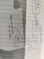
My RF input is a pure sine wave (no modulation). for a single normal operation, I am having the information of frequency based on which I am changing the NCO frequency to get the down-converted baseband signal and using 10*log(I^2+Q^2) to measure the amplitude from the captured I and Q.
now my front-end insertion loss is different for each different frequency. for example, my front end loss is 2 dB for 35 MHz RF input, for which I am adding 2 dB fixed digital gain compensation to get the correct amplitude output.
but when my RF frequency is 135 MHz, my front end loss is 3 dB. that means, my digital gain compensation value should be changed based on the RF input frequency information, right?
what would be the suitable way to do this for this kind of situation?
I am thinking to measure the approximate RF input frequency using the FFT algorithm and based on the measured RF frequency, I will prepare a look-up table for each frequency with respect to the required digital gain compensation value, which will further change the same.
Is there any best way to do above , kindly provide suggestions and feedback.
(FY: Once my RF input frequency changes, it will be constant for one single operation of 2-3 hours)
I am using a high-speed data converter with FPGA to measure the RF signal amplitude and phase. below is my query.
My RF input is a pure sine wave (no modulation). for a single normal operation, I am having the information of frequency based on which I am changing the NCO frequency to get the down-converted baseband signal and using 10*log(I^2+Q^2) to measure the amplitude from the captured I and Q.
now my front-end insertion loss is different for each different frequency. for example, my front end loss is 2 dB for 35 MHz RF input, for which I am adding 2 dB fixed digital gain compensation to get the correct amplitude output.
but when my RF frequency is 135 MHz, my front end loss is 3 dB. that means, my digital gain compensation value should be changed based on the RF input frequency information, right?
what would be the suitable way to do this for this kind of situation?
I am thinking to measure the approximate RF input frequency using the FFT algorithm and based on the measured RF frequency, I will prepare a look-up table for each frequency with respect to the required digital gain compensation value, which will further change the same.
Is there any best way to do above , kindly provide suggestions and feedback.
(FY: Once my RF input frequency changes, it will be constant for one single operation of 2-3 hours)