Continue to Site

Welcome to EDAboard.com

Welcome to our site! EDAboard.com is an international Electronics Discussion Forum focused on EDA software, circuits, schematics, books, theory, papers, asic, pld, 8051, DSP, Network, RF, Analog Design, PCB, Service Manuals... and a whole lot more! To participate you need to register. Registration is free. Click here to register now.

reference voltage of the bandgap reference circuit by using 0.13um CMOS silterra tech

Status
Not open for further replies.

kk913913

Newbie level 3
Joined
Jan 2, 2012
Messages
3
Helped
0
Reputation
0
Reaction score
0
Trophy points
1,281
Activity points
1,304
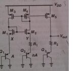
What is the reference voltage for bandgap reference circuit if i'm using 1.2V Vdd ,Silterra 0.13um CMOS tech? ? should be around 1.2V?some of the journals shown around 0.5V for the reference voltage for 0.13um tech.Thank you~
 

One of the key properties of a good bandgap reference circuit is the generation of a reference voltage independent of the Vdd value. Without knowing what kind of bandgap reference you are using I do not think it is possible to say it for sure. But generic references generate something around 1.2 V and that is why they are called bandgap references as the bandgap of silicon is nearly 1.2 eV.

I've designed a bandgap reference in AMS 0.35 technology with topology reported in this paper https://citeseerx.ist.psu.edu/viewdoc/download?doi=10.1.1.85.2694&rep=rep1&type=pdf . It has a very good performance with low Vdd's but it made us to use large resistors as the voltage of AMS tech is 3.3V.

I'll be happy to help if you have questions about this reference circuit.

Edit: The bandgap reference reported in the article generates a 200 mV reference voltage.
 
Last edited:
Thank kemiyun for help,my design is the circuit shown in razavi's book at figure 11.20 ,what do you think for the output voltage ? if using 1.2 Vdd
 

Attachments

  • BG11.20.jpg
    BG11.20.jpg
    11.5 KB · Views: 165

This analysis should be on the book somewhere but let's do it anyway. First in order to keep the transistors in saturation, you require a voltage level of Vth + vdssat for M3 plus Vth + vdssat for M1 and also the Vbe of the BJT. These terms changes with the process but in general Vth = 0.5, and most of the time vdssat in bandgaps are 0.2 to 0.1 V so this circuit may not work at 1.2V supply without modification.

To work with supply voltages as low as 1.2V you should avoid stacking transistors. This kills the supply voltage range. If you are stacking devices anyway, try your best to use wide swing cascode structures.

I haven't searched the literature in detail but I'm not sure you can get out of this without using an OPAMP.
 

Thx for your reply,what kind of modification to make sure all the trans is in saturation with Vdd 1.2 without using stacking transistor?for supply independent.
any recommendation for designing bandgap with Vdd1.2 by using 0.13um silterra tech? ?
 

I do not know what devices the Silterra Tech offers but the bandgap I've already said might be a beginning. Check out the literature there should be many more propositions for solving this problem as it is an important problem for modern circuits. Also the paper I've referred is written by Vadim Ivanov and his group which makes it very trustworthy like all the papers at Journal of Solid State Circuits. There are also some alternatives reported in that paper.

Well the point is to have only 1 BJT and only 1 current source (MOS or BJT doesn't matter) between supplies. To achieve a good current source without cascoding is very hard to do if you are not using an OPAMP (An OPAMP to force the current flow from each side). That was my point in my first post. As you can see that the circuit you referred actually contains a current mirror at the top side. Which forces the currents from each sides to be equal. Doing this with just a simple mirror would be painful in 0.13um tech as the output impedances should be very low, so low that they are not actually a mirror. And this explains why I said that there should be an OPAMP somewhere.
 

Hello kk913913,

The topology you have attached only permits an output voltage reference equal to ~ 1.2 [V]. Therefore, it is impossible to design it using VDD >1.2 [V].(for instance, 1.6 V). Some times, 0.13 um processes have I/O devices whose VDD is nearly 1.8 or 2.5 volts, or even 3.3.Check if you have these devices, if yes, so you can use them and design your circuit.
If the process does not allow for them, you need to change the topology. You can use MOSFETs working in Subthreshold region and then , achieve an output voltage less than 1.2 [v],

Take a look on this traditional topology: A CMOS Bandgap Reference Circuit with Sub-1-V Operation
Hironori Banba, Hitoshi Shiga, Akira Umezawa, Takeshi Miyaba,
Toru Tanzawa, Shigeru Atsumi, and Koji Sakui.

It works for your case.

I hope it helps,
 
Last edited:
Hi kk913913,

I designed bandgap with Vref = 0.5V using 0.18um process. I also followed the paper that palmeiras mentioned above, it gives the good circuit.
And here is my circuit:
bandgap.JPG
Hope this helped!
 
  • Like
Reactions: butchi

    butchi

    Points: 2
    Helpful Answer Positive Rating
hi ducvilla,
can your design work with 1.2V supply voltage?
 

Hi hujiaomianhao,

Totally Yes!

In the first simulation, with Vdd = 1.8V, it can run very well.
And in second one, I try it with Vdd=1.2V, it also has good performance!

^_^
 
hi ducvilla
can you show your detail of the opamp?
as i know,in low supply voltage bandgap,opamp is very especial!
 

Status
Not open for further replies.

Part and Inventory Search

Welcome to EDABoard.com

Sponsor

Back
Top