Continue to Site

Welcome to EDAboard.com

Welcome to our site! EDAboard.com is an international Electronics Discussion Forum focused on EDA software, circuits, schematics, books, theory, papers, asic, pld, 8051, DSP, Network, RF, Analog Design, PCB, Service Manuals... and a whole lot more! To participate you need to register. Registration is free. Click here to register now.

Reducing switching noise in MOSFET inverter

Status
Not open for further replies.

mike buba

Member level 2
Joined
Nov 17, 2013
Messages
50
Helped
0
Reputation
0
Reaction score
1
Trophy points
1,286
Activity points
1,707
Hi, I am trying to reduce switching noise in the MOSFET three-phase inverter.

The reason is that a high noise causes the TI control card serial emulator to reset. I am losing the serial communication connection between the local PC and the control card at higher power. TI engineers advised me to try to use more robust emulators ($$). Before doing that, is there a way to reduce switching noise?

I have already reduced gate resistance (Rgon and Rgoff) by 1/3. The noise reduced, but not significantly. I can try to reduce it even more, but I read this can lead to increased switching losses.

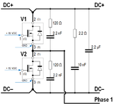
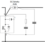
Another option is to add/modify RC snubber. There is already an RC snubber on the board, with an option to add another RC snubber across the lower switch. Should I add RC snubber across the lower switch? I have seen online pictures with only snubber across DC+/- or across each switch in a leg, but my configuration only has an option across the lower leg and/or across DC+/-.
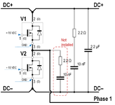
Drawing2.png

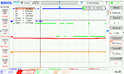
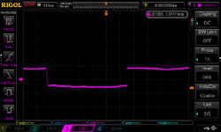
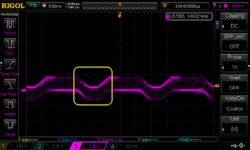
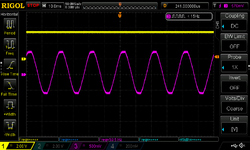
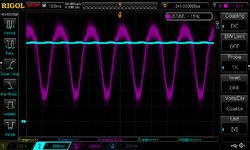
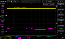
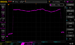
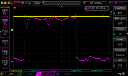
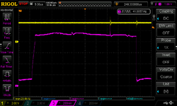
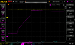
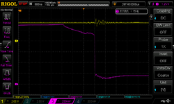
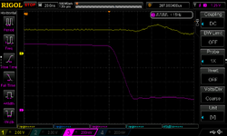
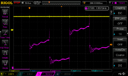
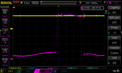
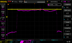
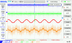
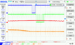
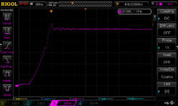
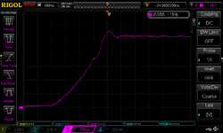
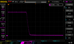
Noise is shown in oscillograms below (different time division: 10 ms, 500 us and 20 us, respectively). I don't see much of a ringing, just a spike at 8 kHz. Also, the inverter switching frequency is 4 kHz, but the noise is at 8 kHz?! Not sure why is that.
Ch1 is Rx signal
Ch2 is Tx signal
DS1Z_QuickPrint20.pngDS1Z_QuickPrint19.pngDS1Z_QuickPrint18.png
 
Last edited:

Solution
Hi,

The most important is a schematic: Where is the source of noise, where to put the filter, which filter.

But almost equally important is the PCB layout. The fancy filter is useless if the PCB layout is bad. A bad PCB layout can make a filter almost useless.

Klaus
Here's a good app note on RC snubbers. Page 2-4 gives simple steps for optimizing R and C experimentally.

Like Easy mentioned it's important for the inductance in your snubbing circuit to be very low, at least much lower than the parasitic inductance which is responsible for the ringing you're trying to dampen. The closer to the drain/source terminals, the better. No wirewound resistors. Leaded film resistors are ok. Old carbon composition resistors actually work very well for snubbing.
 
Hi, I am trying to reduce switching noise in the MOSFET three-phase inverter.

The reason is that a high noise causes the TI control card serial emulator to reset. I am losing the serial communication connection between the local PC and the control card at higher power. TI engineers advised me to try to use more robust emulators ($$). Before doing that, is there a way to reduce switching noise?

I have already reduced gate resistance (Rgon and Rgoff) by 1/3. The noise reduced, but not significantly. I can try to reduce it even more, but I read this can lead to increased switching losses.

Another option is to add/modify RC snubber. There is already an RC snubber on the board, with an option to add another RC snubber across the lower switch. Should I add RC snubber across the lower switch? I have seen online pictures with only snubber across DC+/- or across each switch in a leg, but my configuration only has an option across the lower leg and/or across DC+/-.
View attachment 177074

Noise is shown in oscillograms below (different time division: 10 ms, 500 us and 20 us, respectively). I don't see much of a ringing, just a spike at 8 kHz. Also, the inverter switching frequency is 4 kHz, but the noise is at 8 kHz?! Not sure why is that.
Ch1 is Rx signal
Ch2 is Tx signal
View attachment 177077View attachment 177076View attachment 177075
Try winding few turns (5~6 or more ) of your PC communication cable (USB may be)on an common mode choke toroid core (preferably high perm ), this will reduce common mode current spikes generated from power switching to get coupled to common mode path causing communication loss.
 

keep to 2.2nf at this stage, as for the high side mosfets, if it has to go under the driver - so be it.
--- Updated ---

once the subbers are in place you need a decent high BW scope and probes to look at the mid point - zoom into to 20nS / div or whatever gives you a good look at the transition each way - and post.
After some trial and error and finding the optimal resistors, I put them the closest I could; all under MOSFET drivers. Values are still 2200 pF and 120 ohm.
20220719_203152_2.jpg
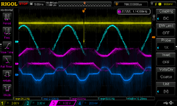
I was able to go to 650 Vdc and I recorded voltage between the leg midpoint and the ground.
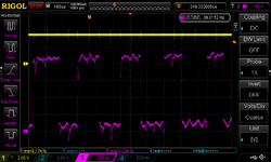
I am still seeing switching noise similar to the previous case. Rgon is still 23.5 Ohm and Rgoff is 10 Ohm.
Ch1 is Rx serial signal
Ch2 is output voltage U-V
Ch3 is leg midpoint to GND
Ch4 is input current (Active PFC is the first stage before MOSFET three-phase inverter)
I suspect that the noise on Rx and Tx signals is close to the SCI chip high/low-level MIN/MAX range, thus accidentally triggering the chip and causing it to stop working. Hence, I am trying to reduce the noise.
DS1Z_QuickPrint45.png
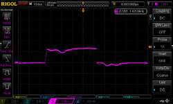
Ch3 zoom (top and bottom section)
DS1Z_QuickPrint46.pngDS1Z_QuickPrint47.png
 

NOW, you need decent decoupling, from Drain top device to source bottom device, say 100nF - min, 800V, leads as short as possible ... on each totem pole ...
--- Updated ---

how do you know your PFC is not making noise ... ?
--- Updated ---

cannot see a full screen zoom in of the totem pole switching at 650 V ... ?
--- Updated ---

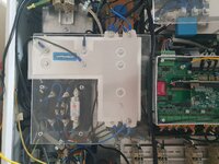
can we see the actual fets please ?
--- Updated ---

if we see the fets, will we also see the extant decoupling ?
 
Last edited:
NOW, you need decent decoupling, from Drain top device to source bottom device, say 100nF - min, 800V, leads as short as possible ... on each totem pole ...
There is already 2.2 uF across upper MOSFET drain and lower MOSFET source.
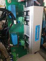
Drawing2.png20220723_150534.jpg
how do you know your PFC is not making noise ... ?
PFC is switching at 20 kHz and the noise is at 8 kHz. Also when I tested only the PFC circuit at 700 Vdc out and full power, the communication was not breaking down and the noise was not visible on the signals on the scope.
cannot see a full screen zoom in of the totem pole switching at 650 V ... ?
I used differential probe x500 to measure the Ch3 signal.

... although, I am now running simulation and at this measuring point should be seeing a PWM signal on the scope, which is not the case as there are periods where voltage drops below zero:
(This is for 400 Vdc, I don't have just this signal for 650 Vdc, only in combination with Ch1, Ch2 and Ch4 as shown in my previous post.)
DS1Z_QuickPrint34.png

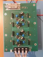
can we see the actual fets please ?
Picture above; the other side is symmetrical.
 
Last edited:
Those caps are a little far away for my liking

I can see CM effect from the PFC stage getting into the purple signal, Ch 3

it appears you need to float your scope ( iso transformer ) so that the scope gnd can be connected to the power ckt gnd. Do not touch the scope when things are running - switch off the power ckt to adjust the time base, volts/div, trig etc
A nice look at each transition 50nS / div or so would be nice, so that the transition occupies 70% of the horiz screen and 80% of the height, also the HVDC pos, w.r.t. gnd - just to make sure it isn't modulated by the PFC too much - various time bases

at 100x prope and 400V, we should see 4V - why isn't this the case ? Oh I see, 500x diff probe - a lot of these are shit for CM and HF transitions ...

There is also a possibility of sw noise from the inv stage interfering with the PFC control

if you are probing control signals at med to high power put a short leaded 4k7 or 10k or 22k as required on the prove tip, with just 1 - 3mm of lead sticking out of the resistor body, resistor body also close to probe tip - this will stop noise being injected into the point you are trying to look at.
--- Updated ---

p.s. for V1, pin 3 is not gnd and should not be labelled such.
--- Updated ---

p.p.s. those 2u2's are only 450V - so risk going poof above 500V.
--- Updated ---

also - once you are bit better organised - you can run a strip of 1mm Al, along under your shubbers ( tie it to 0vHVDC) place Kapton tape under the R's ( you can straighten them a bit ) and superglue the tabs to the Al strip ( i.e. heat flow thru the Kapton ) - this will give good heatsinking up to about 80 deg C ( the glue ).
--- Updated ---

I like your heatsink with clips & fan - is that a standard part ? if so can you fwd a link please ?
 
Last edited:
Those caps are a little far away for my liking

I can see CM effect from the PFC stage getting into the purple signal, Ch 3
When there is no power and no input voltage I can see input voltage on the scope. This could explain why I see this signal superimposed on my PWM signal... though, not sure why I see the AC signal in the first place :confused:
DS1Z_QuickPrint67.png
it appears you need to float your scope ( iso transformer ) so that the scope gnd can be connected to the power ckt gnd. Do not touch the scope when things are running - switch off the power ckt to adjust the time base, volts/div, trig etc
Already have that.
A nice look at each transition 50nS / div or so would be nice, so that the transition occupies 70% of the horiz screen and 80% of the height, also the HVDC pos, w.r.t. gnd - just to make sure it isn't modulated by the PFC too much - various time bases

at 100x prope and 400V, we should see 4V - why isn't this the case ? Oh I see, 500x diff probe - a lot of these are shit for CM and HF transitions ...
Ch2: differential probe x200, DC+ to DC-
Ch3: differential probe x500, DC+ to GND
Same 50 Hz signal superimposed to the DC voltage on Ch3
I have only a set of passive probes up to 300 V (x1 and x10) which came with the scope.
DS1Z_QuickPrint66.png

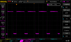
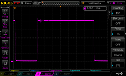
PWM pulses at 500 Vdc; at different time bases and plots.
Ch3: differential probe x500, phase leg midpoint to GND
DS1Z_QuickPrint59.pngDS1Z_QuickPrint63.pngDS1Z_QuickPrint64.pngDS1Z_QuickPrint61.png

At 400 Vdc
DS1Z_QuickPrint56.pngDS1Z_QuickPrint57.png
if you are probing control signals at med to high power put a short leaded 4k7 or 10k or 22k as required on the prove tip, with just 1 - 3mm of lead sticking out of the resistor body, resistor body also close to probe tip - this will stop noise being injected into the point you are trying to look at.
I don't mind the noise in the scope signals.. I suspect that the noise is causing the serial communications interface (SCI) board to trigger and block. If I reduce the overall noise, I wouldn't have to filter scope signals.
I like your heatsink with clips & fan - is that a standard part ? if so can you fwd a link please ?
https://www.fischerelektronik.de/web_fischer/en_GB/heatsinks/D02/Miniature cooling aggregates/$catalogue/fischerData/PG/LAM4K/
please tell me this cap is not across C-E on the IGBT in the booster

View attachment 177573
This is the schematics. There is a nylon standoff on IGBT boost diode and on the top, there is a common connection for capacitor, diode and output.
Drawing3.png
 
Last edited:
OK - several things are now evident

- the turn on is still way too fast on the inverter fets, causing dv/dt of greater than 400V in 20nS ? - the edge is still not zoomed in enough - the transition ( e.g. hi to low or vice versa ) should be 80% of horiz. - I take it English is not your 1st language - no worries.

- there is not enough C on the bus, by quite a margin - are there any electro's on the HVDC ?

- the diff probes are not very flash at all - probably the leads are too long - and they will radiate, esp if on a switch node - they are probably isolating though - check - you can then unfloat your scope.

- the point of having R's on scope probes is to stop noise going into the control ckt when you probe it - not any other reason.

- buy some 100x probes.

- form a shorted loop with a x1 or x10 scope probe, gnd lead to tip, wind down the V/div as you wave it around the power ckt to find the largest signal, I expect it will be from the booster, but if it is from the inverter fets, slower turn on will help ... this is the largest di/dt noise source.

you can do the same with a 1" insulated stub - basically the scope probe with the gnd lead ( wire going to the croc clip ) removed - to find the highest dv/dt point - likely the inverter stage.

Afew turns of the scope probe wire - near the BNC end - around a power ferrite toroid will help limit CM pick up if the probes are long enough to do this.

PLease check if the cap is across the C-E of the IGBT - it certainly looks it - OK I see it is lifted from the old post.
--- Updated ---

edit: I see the cap on the booster IGBT is lifted by a steel standoff ( brass better - as the steel forms a slightly lossy inductor ) so not across the C-E, thank fully.
 
Last edited:
OK - several things are now evident

- the turn on is still way too fast on the inverter fets, causing dv/dt of greater than 400V in 20nS ? - the edge is still not zoomed in enough - the transition ( e.g. hi to low or vice versa ) should be 80% of horiz. - I take it English is not your 1st language - no worries.
Recordings with Rgon = 47 Ohm, at 500 Vdc
One switching event
DS1Z_QuickPrint75.png
Turn on (zoomed)
DS1Z_QuickPrint76.png
Turn off (zoomed)
DS1Z_QuickPrint77.pngDS1Z_QuickPrint78.png

Should I be increasing the Rgon even more, or should I increase snubber capacitance?

Btw. this reference says to add RC snubber across low-side MOSFET.

- there is not enough C on the bus, by quite a margin - are there any electro's on the HVDC ?
There are two electronic capacitors (400 V, 4700 uF) in series n the DC bus.
- the diff probes are not very flash at all - probably the leads are too long - and they will radiate, esp if on a switch node - they are probably isolating though - check - you can then unfloat your scope.

- the point of having R's on scope probes is to stop noise going into the control ckt when you probe it - not any other reason.

- buy some 100x probes.
A little pricey 🙁. This one is below £100, others are above £250 or even more
- form a shorted loop with a x1 or x10 scope probe, gnd lead to tip, wind down the V/div as you wave it around the power ckt to find the largest signal, I expect it will be from the booster, but if it is from the inverter fets, slower turn on will help ... this is the largest di/dt noise source.
I use a current probe and place it above the circuit and the board to see what is the biggest source of the noise. There is noise coming from boost IGBT and some from inductor... But when looking at the scope, the noise frequency is 8 kHz (PFC is 20 kHz and Inverter is 4 kHz).
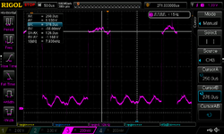
This is recorded with the converter deblocked, but no input voltage (both PFC and inverter pulses were on); spikes in Rx signal (Ch1) are at 8 kHz.
DS1Z_QuickPrint52.png
 

If I measure the ringing frequency, especially visible during the turn-off period on the yellow signal (Ch1), I get fringing0 = 10 MHz. So to reduce the ringing frequency, I should be increasing capacitance.
I can assume that the current capacitance in the circuit is equal to or higher than the existing RC snubber capacitance 2200 pF (assuming existing unknown parasitic capacitance < existing RC snubber capacitance 2200 pF). Hence, to reduce the ringing frequency, a new capacitance has to be higher than 2200 pF.

fringing0=1 / (2π√L0×C0)​

Adding a capacitor, the ringing frequency will change from fringing0 to fringing1, where

x = fringing0 / fringing1

From there, a required Cadd can be calculated as:

C0 = Cadd / (x2−1)​

source
Further calculation using the same source gives Rsnubber = 3.62 Ohm

Using this source (Ipk = 6, rt = 1.5 us, Vrail = 650 and F = 4 kHz), Csnubber is calcualted as 13.846 nF and Rsnubber is 900 Ohm, 12 W. Similar Csnubber values, but 250 times higher Rsnubber :(


Also, some references suggest adding RC snubber across the low-side MOSFET.
Not sure what is the advantage or disadvantage of adding across both vs only lower.


I assume the spikes during the conduction period are because other legs are switching and this affects this signal.
DS1Z_QuickPrint70.pngDS1Z_QuickPrint75.png
 
Last edited:
from your reference:
- note the last line of text ( you really need better references )
1658721897668.png


even the formula is wrong.
--- Updated ---

the traces show 500VDC in ~ 25nS, or 20,000 V / uS on the inverter fets under some parts of the ac output cycle - at turn on.

Now you see why noise is every where. This pretty high dv/dt couples into the heatsink and down the output wire and gets onto and into everything - kicking resonances on other ckts into action - hence the ringing on the yellow trace.

p.s. re your current probe - current cannot change instantaneously ( infinite volts needed ) so the waveform observed is in fact dv/dt from the fet turn on in the inverter - i.e. your current probe is not shielded against dv/dt pick up. N.B. a fet ( not the same one ) turns on twice in a 4kHz cycle => hence 8kHz noise. For a 3 phase output ( i.e. 3 totem poles ) you would expect to see 12kHz & 24kHz noise, if the turn off is soft the 12kHz will dominate.

The turn on gate resistors should be raised to say 150 ohm - see if this makes a big difference.

Forgive me for saying this - but the transitions show no ringing - so the above snubber calcs can go in the round filing receptacle. I.e. the snubber values are pretty perfect as they are - if a trifle on the light side.

You need to get the 2u2 caps - or better yet get some others a bit skinnier, right onto the D-S HVDC of each totem pole - so 3 caps, do what it takes to get them in there on V short leads, 100nF to 470nF film/foil, ideally 630VDC ( this will let you get to 650V )

The 450V 2u2's are a worry if you go to 650V - they may hack it - they may not. They can partially break down internally ( some are self healing to an extent ) and make some really good random RF and audible noise as they break down internally and swell up - worst case they blow up and take out an eye.

The electro's need to be as close as possible to the fets too - as they add damping to the HVDC bus, so cut and paste and hack and saw to get them nearby, or some new ones, e.g. 220uF, 400V, each - SHARING resistors are imperative - else the electro's will make a really loud noise and telescope and take out more than just an eye. at 325V say, 220k 3W across each to hack the volts and the 1/2 watt dissipation.

I would expect gruntier snubbers will be the salvation in the end - you can use the TO-220 clips to clip the R's to the heatsink ( very handy ...! ) and add caps.

Leave the existing snubbers in, but add say 3n3 & 220 ohm ( 5.6 watt on the TO-220 ) across each device - if this is needed.

If the fets can survive turn on losses at 150 ohm gate Ron, then extra snubbing may not be required - time to experiment with Ron.

You can use your " current probe " to see if the RF noise diminishes, as well as the turn on transition speed of the inverter fets.
--- Updated ---

This is recorded with the converter deblocked, but no input voltage (both PFC and inverter pulses were on);

What does the above mean ? deblocked? with no Vin there will be no noise .. ?

the statement is pretty non sequitur.
 
Last edited:
Oh, can we see the Vce on the boost IGBT at peak current turn off please ? 20 -50nS / div, full height on screen.
--- Updated ---

Oh - and turn on ... too, please.
 
Last edited:

The turn on gate resistors should be raised to say 150 ohm - see if this makes a big difference.
I'll order 82R and 100R and see how it goes first. step by step
Forgive me for saying this - but the transitions show no ringing - so the above snubber calcs can go in the round filing receptacle. I.e. the snubber values are pretty perfect as they are - if a trifle on the light side.
I was looking at the turn off period and measuring oscillations on the yellow signal.
You need to get the 2u2 caps - or better yet get some others a bit skinnier, right onto the D-S HVDC of each totem pole - so 3 caps, do what it takes to get them in there on V short leads, 100nF to 470nF film/foil, ideally 630VDC ( this will let you get to 650V )

The 450V 2u2's are a worry if you go to 650V - they may hack it - they may not. They can partially break down internally ( some are self healing to an extent ) and make some really good random RF and audible noise as they break down internally and swell up - worst case they blow up and take out an eye.
Smaller one directly on MOSFETs DC+/-: https://uk.rs-online.com/web/p/products/8752144/
Bigger 2.2 uF replacement for existing 450 V: https://uk.rs-online.com/web/p/products/8829391/

No idea how to put smaller under the drivers, next to RC snubbers :confused:
I have to leave some creepage distance as well
The electro's need to be as close as possible to the fets too - as they add damping to the HVDC bus, so cut and paste and hack and saw to get them nearby, or some new ones, e.g. 220uF, 400V, each - SHARING resistors are imperative - else the electro's will make a really loud noise and telescope and take out more than just an eye. at 325V say, 220k 3W across each to hack the volts and the 1/2 watt dissipation.
Already have that. I can add another paraller branch (2 in series 4700 uF, 400 V) branch.... is 220uF an error in writing or there should be really 4700 uF in paralle with 220 uF for DC bus link?
I would expect gruntier snubbers will be the salvation in the end - you can use the TO-220 clips to clip the R's to the heatsink ( very handy ...! ) and add caps.

Leave the existing snubbers in, but add say 3n3 & 220 ohm ( 5.6 watt on the TO-220 ) across each device - if this is needed.
Not sure how to do that? I simply don't have any ideas on how to add new RC snubber in parallel with this one 🤔 /open to suggestions :) / and there is also capacitor there as well 😓.

Even now all looks so cramped. I am not even thinking about adding a heatskink. If they were on the side of the driver, I could add one for each resistor. Now, with my current knowledge and skills, two parallel RC snubber branches and capacitor across... it simply doesn't fit under.

The best Ican think of now is to replace existing 2.2 nF with 4.7 nF or 6.8 nF and leave 120 Ohm, 35 W resistor. or oven reduce resistance to 77 Ohm (120 Ohm || 220 Ohm)?

I will send boost turn on/off oscillograms shortly.
 

220uF are smaller and can hopefully get closer to the inverter fets

4700uF will have a low SRF and are just inductors for ringing frequencies - hence the very non flat HVDC line.

the yellow signal is not a totem pole output - it is merely a line ( undefined ) that is getting kicked into ringing

snubbers are always problematic when you don't design for them from the off

hopefully the slower turn on will be enough of a solution

the boost waveforms will be instructive I think
--- Updated ---

I note the fixed 1.5uS dead time - you can see that at the instant of true turn off where the voltage wanders up to the pos rail - there is very little disturbance of the yellow trace. Only when a mosfet turns on, is the high dv/dt generated and then kicks the yellow trace into a ringing oscillation.
 
Last edited:
Active PRC at 500 Vdc output voltage, turn on and turn off waveforms across boost IGBT... though, not sure if managed to I capture it at the peak current.
Differential probe x500
Switching period (several and one)
DS1Z_QuickPrint84.png DS1Z_QuickPrint80.png
Turn on (different time base)
DS1Z_QuickPrint81.png DS1Z_QuickPrint82.png
Turn off
DS1Z_QuickPrint83.png
 
Last edited:

how is this project progressing - 650V ?
It took some time and work, but I finally got to 650 Vdc link voltage. As a last acttion, I was looking at how to reduce inductance in the DC link and did some major rearrangements.
20220827_171233.jpg

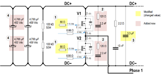
Here is a summary of work and modifications:
  1. Increased Rgon from an initial 6.66 Ohm to 80 Ohm.
  2. Added RC snubber across each MOSFET (2,2 nF and 120 Ohm).
  3. Increases DC link capacitance across inverter leg from 2.2 µF to 3.3 µF, 900 Vdc
  4. Increased DC link capacitance by adding a new parallel branch with two 4,700 µF in series.
Drawing2.png
There is still some noise in the signal, but the communication does not break anymore at 650 Vdc. I've been running it for a few days and all looks ok.
If the communication starts breaking again, I have also bought 100 Ohms and 120 Ohms, if I need to increase Rgon. I also have 4,7 nF to add in parallel to the existing RC snubber or replace 2,2 nF.


Thank you very much for your advice and suggestions.
 

Status
Not open for further replies.

Similar threads

Part and Inventory Search

Welcome to EDABoard.com

Sponsor

Back
Top