Continue to Site

Welcome to EDAboard.com

Welcome to our site! EDAboard.com is an international Electronics Discussion Forum focused on EDA software, circuits, schematics, books, theory, papers, asic, pld, 8051, DSP, Network, RF, Analog Design, PCB, Service Manuals... and a whole lot more! To participate you need to register. Registration is free. Click here to register now.

[Recommend the stackup and layers for HDI PCB ]

Status
Not open for further replies.

k621219

Newbie level 6
Joined
Apr 2, 2009
Messages
12
Helped
0
Reputation
0
Reaction score
0
Trophy points
1,281
Activity points
1,367
[Recommend the stackup and layers for HDI PCB ]

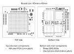
I am designing the PCB for BGAs at double side.

**broken link removed**

I think that it will need to use HDI PCB.
It is first time to do HDI PCB design.

It is difficult to decide the layers and stackup.

I am considering about the following spec.

- 3 + N + 3 type stackup, 10 ~ 16 layers.
- stacked microvias

Please recommend the the layers and stackup by your experience about HDI PCB design.
 

I missed the image link.
 

Attachments

  • two_side.JPG
    two_side.JPG
    53.2 KB · Views: 81

Your going to have some fun, especially length matching the DDR.
I agree HDI is the best option, though for cost purposes I would go for non stacked microvia's. I also find non stacked to be a bit easier to visualise during the design stage so I know how far down the layer stack I am (also most of the HDI designs I do are non-stacked due to the afore mentioned cost factor).
Without knowing all the details of the circuit such as power supplies etc. it is hard to comment on a layer stack up and with the density of routing again a definitive answer is hard to give. I would try a few stack ups and see what routing area you are left with, the DDR memory being critical...
But looking at the layout, you are not going to be able to place decoupling caps in the correct positions so for this design I would go with the next layer down from the components as GND, then the next layer as the supplies so you get a closely coupled plane layer next to the components on each side of the board, with as much planar capacitance as possible to cater for the decoupling (or lack of it in your case). This will also minimise the loop area for the power supplies again having benefits.
 

Thank so much for your advice.

Now I have price problem.
I have received several quotations for HDI PCB fabrication.

- Board size: 40 mm x 40mm
- Quantity : 4
- Layer : 12
- Build-up PCB (HDI PCB): 3-6-3 (12 layers)
- Blind via: L1-L2, L2-L3, L3-L4, L9-L10-, L10-L11, L11-L12
- Buried via : L4-L9
- stacked microvia

In Korean PCB manufacturer, the prices was almost four times higher (about USD 2,700) than standard PCB (about USD 700).

For cost down, I requested new quotation for the following spec.
- Board size: 40 mm x 40mm
- Quantity : 4
- Layer : 10
- Build-up PCB (HDI PCB): 1-8-1 (10 layers)
- Blind via: L1-L2, L2-L3, L8-L9, L9-L10
- Buried via : L2-L9
- staggered microvia

In a Korea PCB manufacturer, the prices was almost three times higher (about USD 2,000) than standard PCB (about USD 700).

In a China PCB manufacturer, the prices was almost two times higher (about USD 1,400) than standard PCB (about USD 700).

With stacked via and more two lamination, the different price is about USD 700.
I think that the different price is small than I thought.
Just simpe HDI PCB stackup, the price is about three times.
Is it normal case ?

How do you think about the 1-8-1 (10 layers) stackup for the PCB design ?
Do you think that it is possible ?
I have a few PCB design experience and also it is first time for HDI PCB design.

Now I are going almost to give up HDI PCB design because of PCB fabrication cost.
 
Last edited:

I am surprised at the cost differences and would hope this would improve as HDI is fast becoming a necessity for many designs. I have done similar boards to yours and have had to use HDI because there was no other option due to space, I will try and find one time permitting and look at whet stack up was used, the problem being none had DDR memory on so whilst dense didn't have all the timing issues to sort out.
 

Status
Not open for further replies.

Part and Inventory Search

Welcome to EDABoard.com

Sponsor

Back
Top