Welcome to our site! EDAboard.com is an international Electronics Discussion Forum focused on EDA software, circuits, schematics, books, theory, papers, asic, pld, 8051, DSP, Network, RF, Analog Design, PCB, Service Manuals... and a whole lot more! To participate you need to register. Registration is free. Click here to register now.
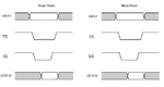
In the picture that I have attached I am confused about the white and grey shaded areas. Is the grey region where data/address is ready to be read or is the white region
according to picture the data to be read is in white area. as CS and RD and WR active low signals allow chips to read and write data during white regions. while gray regions are ignored for that specific chip. data not alined under signals is due to some propagation delay or respond time of the device after recieving the signal.
This site uses cookies to help personalise content, tailor your experience and to keep you logged in if you register.
By continuing to use this site, you are consenting to our use of cookies.