Continue to Site

Welcome to EDAboard.com

Welcome to our site! EDAboard.com is an international Electronics Discussion Forum focused on EDA software, circuits, schematics, books, theory, papers, asic, pld, 8051, DSP, Network, RF, Analog Design, PCB, Service Manuals... and a whole lot more! To participate you need to register. Registration is free. Click here to register now.

radiated emission SEPPIC 24W

Status
Not open for further replies.

seridj_mse

Member level 2
Joined
Jan 18, 2021
Messages
53
Helped
0
Reputation
0
Reaction score
2
Trophy points
8
Activity points
311
HI,

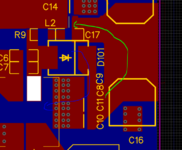
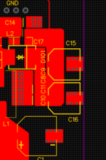
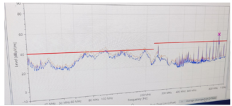
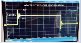
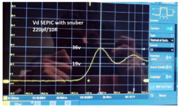
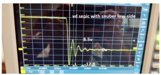
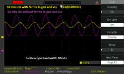
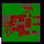
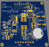
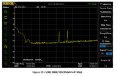
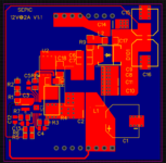
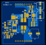
We have tested our equipment SEPIC DC DC input:9-30V output : 12V/24W (PCB 2LAYER) for CISPR 16 radiated emission limits. The emission result is attached. I have trouble shooted the problem element.

for pics i know its about quartz 50Mhz but the probleme is with renonant , i tried with RC , and RDC snubber but i cant solve probleme


1663863275669.png
1663863302218.png
 

Mind the "slot" between green and cyan to guide the signal.
i didnt understand well what u want i do . its the same area i cant see the slot ...

here is the update of layout without gnd plan in top and with only one piste in bottom :
 

Attachments

  • 1664374938000.png
    1664374938000.png
    137.5 KB · Views: 85
  • 1664375012951.png
    1664375012951.png
    93.8 KB · Views: 85

i didnt understand well what u want i do . its the same area i cant see the slot ...
loop_n2.PNG

Now the slot (or call it gap) is in blue.
Dirty signal coming from diode
(is prevented by the slot to directly go ot L2)
it has to go to the capacitors
and now as "clean" signal on the right side up to L2
This is not the most elegant solution, but let´s see how it works.

Just to clarify:
cyan sketches the "dirty" signal flow
green sketches the clean signal flow
blue is a slot / gap -> no copper

But looks good now. .. for my taste.
I personally don´t like the non_45° angles. But technically it makes no difference.

Klaus
 

hi , i want to share the result of testing in laboratorie electromagnetic compatibility with modification (diode ,snubber). its better so with modification of PCB layout i think its will be more better. for 50 MHz harmonic its become from mother board , i use the sepic converter in mother board).


Attachments

  • 1664783957298.png
    1664783957298.png
    798.3 KB · Views: 85
  • 1664784436467.png
    1664784436467.png
    765.8 KB · Views: 76
  • SEPIC vd with modification.PNG
    SEPIC vd with modification.PNG
    795.8 KB · Views: 73
  • vd sepic with modification low side.PNG
    vd sepic with modification low side.PNG
    653 KB · Views: 88
by the way , to reduce harmonics of oscillator 50Mhz : https://www.mouser.fr/datasheet/2/122/ecs-2325-2333-8384.pdf

i use bead ferrite in Vcc and/or GND with impedance at 100Mhz : 470R or 600R its good or i should use 1k ? and its normal when i add ferrite Vmax and Vmin of 50mhz siganl change ?
 

Attachments

  • DSO00001.png
    DSO00001.png
    12.5 KB · Views: 84
Last edited:

hi, i jute test my new pcb 2 layer and 4 layer and there is no différence , i have a huge difference when i change ref of diode and mosfet so the emission source its not come from return path and switching nodes with high dV/dt....
 

Attachments

  • 1666004695184.png
    1666004695184.png
    106.5 KB · Views: 64
  • 1666004721451.png
    1666004721451.png
    66.6 KB · Views: 71

Hi,

please give more detailed information:

How did you test. What tests did you compare against each other? What does "change ref of diode" mean?

Klaus
 

Hi,

please give more detailed information:

How did you test.
u can see POST#10 , i test my sepic 24W with input 12v and output 12V@1A and i see the result with spectrum analyzer ....

What tests did you compare against each other?
my old pcb layout with my new pcb with ur help POST#36
What does "change ref of diode" mean?
See POST#16


for resume :

spectrum for my old pcb layout with B360B diode : https://docs.rs-online.com/e459/0900766b814cae4f.pdf and with MOSFET : BSC093N04LS G : https://www.infineon.com/dgdl/BSC09...0107c&fileId=db3a30431689f4420116c44a1fa80822 and without resistor gate .


1666010457436.png


spectrum for my old pcb layout with MBRS3100T3G diode and without gate resistor.


1666012409850.png


spectrum of my new pcb layout 2 layer with same diode and mosfet it's a little worst in tow pics and better in 350mhz .

2.png


spectrum of my new pcb layout 4 layer with same diode and mosfet.

44.png

spectrum of my new pcb layout 2 layer with same diode and mosfet with 50R resistor gate mosfet ( i think me its a big value i use it only for test, for me good value is 5R .... )


4.png


my objective is to keep signal belew -40db.

--- Updated ---

i think i know what i should optimized .... i see both PCB layout had a same high frequency loop that why i didnt get any change in noise .
 

Attachments

  • 1666010936011.png
    1666010936011.png
    156.6 KB · Views: 70
Last edited:

Hi,

In post#10 there are a lot of pictures with different situations.

Two basic questions:
* did you pass EMI tests or not?
* is your test method (sensor, equippment, filters, distances, chamber ... ) according test standards?

I mean: you always get higher "noise level"
* the more close your "sensor" is at the signal
* and the more far is the return path (less compensation)
And the diode will have influece on dI/dt and ringing (maybe caused by reverse recovery problems).

But in the end I don't expect the diode selection to cause an EMI test to fail.

Klaus
 

Two basic questions:
* did you pass EMI tests or not?
No only test with my spectrum analyzer !

* is your test method (sensor, equippment, filters, distances, chamber ... ) according test standards?
yes i try to put my near-field optical probe at same place and distance from SELF


But in the end I don't expect the diode selection to cause an EMI test to fail.
yes

so what is strang is with all modification layout pcb 2 layer and 4 layer i can see i dont have any improvement , i think i reduce loop when mosfet is ON and OFF but the high frequency loop (during the reverse recovery time, hight frequency current flows backwards through the diode node ) is the same in both pcb layout , so i will test with new pcb and i see if i have right ....
 

Hi,

No only test with my spectrum analyzer !
Did you at least try to pass an EMI/EMC test?

yes i try to put my near-field optical probe at same place and distance from SELF
I don´t understand at all. Optical? SELF?

Please tell me the number of the standard.

***
In near field you will always see "noise". It is impossible to zero it.
But this depends a lot on the used HF probe (electric, magnetic, size ....) and on the distance and orientation.

***
The layout is meant to pass EMI/EMC tests. It will reduce emitted noise of the PCB but also noise emitted by the wiring.
Input as well as output ripple should be reduced.

***

my objective is to keep signal belew -40db.
* db? referenced to what?
* or dBm as shown in the scope?

****
spectrum of my new pcb layout 2 layer with same diode and mosfet with 50R resistor gate mosfet ( i think me its a big value i use it only for test, for me good value is 5R .... )
Why do you see 5R is bbetter than 50R?
Did you do an efficiency test?

Klaus
 

Hi,


Did you at least try to pass an EMI/EMC test?
No i didnt , bcs i have the same siganl in scope i will have same result in labo test, so i try to reduce level of dbm and i will pass test in labo ....
I don´t understand at all. Optical? SELF?
i mean for all scope shared i put near-field probe like this, above the coupled inductor

1666085745504.png


Please tell me the number of the standard.

radiated emission CISPR 16-2-3 [30Mhz-1Ghz].


***
In near field you will always see "noise". It is impossible to zero it.
But this depends a lot on the used HF probe (electric, magnetic, size ....) and on the distance and orientation.
yes i know but i will reduce my level noise from -10dbm to -40dbm and i will pass test in labo ...
***
The layout is meant to pass EMI/EMC tests. It will reduce emitted noise of the PCB but also noise emitted by the wiring.
Input as well as output ripple should be reduced.

***
ok

* db? referenced to what?
* or dBm as shown in the scope?

yes i mean dbm on scope !!
****

Why do you see 5R is bbetter than 50R?
Did you do an efficiency test?

Klaus
 

Hi,

i mean for all scope shared i put near-field probe like this, above the coupled inductor
.. and the according picture.

It doesn´t look like a standardized probe.
Also what are the blue and brown thick wires? I guess they make things worse.

I can´t find much information about CISPR 16-2-3 (DIN EN 55016-2-3) equippment. It seems they use a ring antenna in a distance of 3m for near field measurements.
Very different to your method.

Klaus
 

Hi,


.. and the according picture.

It doesn´t look like a standardized probe.
yes, its not standardized at all i made myself


Also what are the blue and brown thick wires? I guess they make things worse.

its only for test diode, i dont use theme in my shared result scope.

Very different to your method.
yes of corse its diffrent ,

for exemple i know with this scope i am so far from limit so that why i want reduce this trace under 40dbm and i will pass in labo to test again ....

 
Last edited:

You will always measure noise directly on the top of the coupled inductor as the shield is typically poor so they will radiate. It is likely one of the biggest sources of magnetic fields. I did mention previously that you may have to cap the inductor with some foil and connect it to your 0V to reduce the radiated emissions as this will likely manafest itself as common mode emissions which would be more difficult to attenuate without a metal box of some sort. I'm also of the opinion that your input power lines (input especially) are likely to have the switching currents on also due to to lack of series impedance so these wires could well radiate also.
 

Hi,

as far as I understand now, you are doing non standard test with non standard equippment.

So far so good.

I also see you are focussed on the diode current, which causes the magnetic field radiation.
Then still my question is:
Why not 50 Ohm? It slows down dV/dt and thus dI/dt and thus improves noise. Clearly can be seen on the test results.
I see no information why you think 5 Ohms still is better than 50 Ohms.
One problem might be decreased efficiency. Thus I aksed about it.

Klaus
 

You will always measure noise directly on the top of the coupled inductor as the shield is typically poor so they will radiate. It is likely one of the biggest sources of magnetic fields.
YES i know , with my probe i have only image of noise and i work to reduce this noise below -40dbm to pass test.
I did mention previously that you may have to cap the inductor with some foil and connect it to your 0V to reduce the radiated emissions as this will likely manafest itself as common mode emissions which would be more difficult to attenuate without a metal box of some sort.
yes of corse it will reduce noise but how i can add this foil in my borad for industrial use and how its cost ....

I'm also of the opinion that your input power lines (input especially) are likely to have the switching currents on also due to to lack of series impedance so these wires could well radiate also.
i dont know but with my prope i dont have any noise in input/output lines ....
--- Updated ---

Why not 50 Ohm? It slows down dV/dt and thus dI/dt and thus improves noise. Clearly can be seen on the test results.
I see no information why you think 5 Ohms still is better than 50 Ohms.
yes its decreased efficiency my input plage is from 9V to 30V and outout 12v@2A , so what i saw with 9V i have 110mA more and with 12V i have 90mA ....
 
Last edited:

Status
Not open for further replies.

Part and Inventory Search

Welcome to EDABoard.com

Sponsor

Back
Top