Continue to Site

Welcome to EDAboard.com

Welcome to our site! EDAboard.com is an international Electronics Discussion Forum focused on EDA software, circuits, schematics, books, theory, papers, asic, pld, 8051, DSP, Network, RF, Analog Design, PCB, Service Manuals... and a whole lot more! To participate you need to register. Registration is free. Click here to register now.

questions about miller-compensation and LDO design

Status
Not open for further replies.

lhlbluesky

Banned
Joined
Mar 30, 2007
Messages
558
Helped
5
Reputation
10
Reaction score
5
Trophy points
1,298
Location
china
Activity points
0
i have some questions need your help, some of these may be simple, but i want to discuss more deeply.
1, in HV process, i see an inverter like the following picture shows, the resistor may be 100K or some other value. what is the role of the resistor? and how it works?
inv.jpg
2, in two-stage miller compensated opamp, nulling resistor is needed to compensate the RHP zero. in some cases, the Rz is not needed, however. i want to know. when can Rz be removed, and using only a Cc for compensation? in my opinion, when CL is very small, Rz can be removed. but why? any other cases?
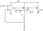
3, in the following picture, a ldo is showed.
first, how to analyze the AC characteristic of the loop? what place is the poles (dominant and non-dominant) and zeros located? and how to stablize the loop? here, we assume two cases: CL=1uF and CL=10pF, and Rc is large (may be 200K~500K), current of opamp is very small.
second, how to analyze the PSRR+ characteristic? in allen's book, a two-stage miller compensated opamp (without Rc and R1, CL is relative small) is analyzed, there is one pole and two zeros in allen's book. when Rc and R1 added, we assume two cases also: CL=1uF and CL=10pF, what is the place of poles and zeros? if i want to improve the PSRR+ of low frequency to 100KHz, what should i do? in my opinion, DC gain and dominant pole both need to be large enough, so the DC gain of opamp and the resistance of the upper PMOS can be increased to improve PSRR+, but in allen's book, when increasing the upper PMOS resistance, the two(DC gain and dominant pole) is changed in opposite direction (assuming low current consumption is required here). so, how to improve the PSRR+ of low frequency to 100KHz here? what other ideas? assuming i want PSRR+ to be 25dB at 100KHz.
third, if i use the circuit as a V-I converter, to get an accurate ref current, how to decrease the mismatch of current mirror caused by vds difference? i know, cascode may be a solution, but cascode current mirror may increase the current consumption, and low current consumption is required also here. what other ideas or solutions? if i use cascode, what is the solution of current-minimized?
the last, in the circuit, CL is relative to GND, but in some cases, CL is relative to VDD, and in some cases, two of both is added. what is the difference of the two (CL relative to GND and relative to VDD)?
ldo.jpg
4, in the following pdf, a BPF is mentioned with a external resistor to tune the center frequency f0. but how is this realized? i have checked some papers, but have no ideas yet. can anyone give me some suggestions or advice? it will be very appreciated, thanks.
bpf.jpg
View attachment U2538B.pdf

any advice will be appreciated, thanks in advance.
 

in the above ldo circuit, if i add two CL=10pF to the output, one is relative to VDD, the other is relative to GND, then, for AC, PSRR and TRAN simulation, what is the equivalent cap loading? in my opinion, that is, 20pF for AC, 10pF for PSRR and 10pF for TRAN, am i right?
 

I think it counts as 20pF in any AC resp. time domain case (where GND & VDD are considered short-cut).
 

but in psrr simulation, vdd is the input, not virtual ground.
besides, what ideas about the questions above i mentioned?
thanks.

- - - Updated - - -

and have anyone used the chip of u2538b? i want to know the BPF structure of it. how to tune the center frequency f0 only using a single external resistor?
 

ok, thanks. and have anyone looked at my above questions 2 and 3?

- - - Updated - - -

and about the BPF in u2538b, any other ideas?
 

Re: output capacitance for PSRR analysis

but in psrr simulation, vdd is the input, not virtual ground.

Right. However, imagine your PSRR s(t)imulation bench: You're using a vdc and a vac source in series, both with zero (or perhaps very low) series resistance. So your vdd input is still virtual ground, in reference to the output.
 

what ideas about my other questions?
besides, for basic BANDGAP core (VBE+deta(VBE) structure using two bjt, a resistor, two PMOS, an opamp to force Vip=Vin), how to analyze the PSRR+? in my simulation, in 30KHz or so, two poles appear (close to each other), and the PSRR+ becomes positive, that is, vo/vdd>1 in some frequency range, why? what is the possible reasons?

- - - Updated - - -

'You're using a vdc and a vac source in series, both with zero (or perhaps very low) series resistance. So your vdd input is still virtual ground, in reference to the output.'
i don't understand well. vdd is ac input, so, it is not ac=0 point, why is it virtual ground? please explain to me more clearly, thanks.

In simulation test benches, all voltage sources have zero series resistance!
 

i have some questions need your help, some of these may be simple, but i want to discuss more deeply.
1, in HV process, i see an inverter like the following picture shows, the resistor may be 100K or some other value. what is the role of the resistor? and how it works?
View attachment 79865
2, in two-stage miller compensated opamp, nulling resistor is needed to compensate the RHP zero. in some cases, the Rz is not needed, however. i want to know. when can Rz be removed, and using only a Cc for compensation? in my opinion, when CL is very small, Rz can be removed. but why? any other cases?
3, in the following picture, a ldo is showed.
first, how to analyze the AC characteristic of the loop? what place is the poles (dominant and non-dominant) and zeros located? and how to stablize the loop? here, we assume two cases: CL=1uF and CL=10pF, and Rc is large (may be 200K~500K), current of opamp is very small.
second, how to analyze the PSRR+ characteristic? in allen's book, a two-stage miller compensated opamp (without Rc and R1, CL is relative small) is analyzed, there is one pole and two zeros in allen's book. when Rc and R1 added, we assume two cases also: CL=1uF and CL=10pF, what is the place of poles and zeros? if i want to improve the PSRR+ of low frequency to 100KHz, what should i do? in my opinion, DC gain and dominant pole both need to be large enough, so the DC gain of opamp and the resistance of the upper PMOS can be increased to improve PSRR+, but in allen's book, when increasing the upper PMOS resistance, the two(DC gain and dominant pole) is changed in opposite direction (assuming low current consumption is required here). so, how to improve the PSRR+ of low frequency to 100KHz here? what other ideas? assuming i want PSRR+ to be 25dB at 100KHz.
third, if i use the circuit as a V-I converter, to get an accurate ref current, how to decrease the mismatch of current mirror caused by vds difference? i know, cascode may be a solution, but cascode current mirror may increase the current consumption, and low current consumption is required also here. what other ideas or solutions? if i use cascode, what is the solution of current-minimized?
the last, in the circuit, CL is relative to GND, but in some cases, CL is relative to VDD, and in some cases, two of both is added. what is the difference of the two (CL relative to GND and relative to VDD)?
View attachment 79866
4, in the following pdf, a BPF is mentioned with a external resistor to tune the center frequency f0. but how is this realized? i have checked some papers, but have no ideas yet. can anyone give me some suggestions or advice? it will be very appreciated, thanks.
View attachment 79867
View attachment 79868

any advice will be appreciated, thanks in advance.

1 - the resistor slows down the falling transient of OUT so this inverter has a skewed delay. When IN goes low OUT goes high very fast and when IN goes high OUT goes low slowly determined by the resistor and the next stage capactiance.

2 - Without the Rz the RHP zero is given by gm/C. If C is sufficiently small and your gm/C is very high much higher than your Gain Bandwidth then the zero does not harm your stability and you don't need to push it out further by adding Rz.

3 - To analyze the AC characteristics one way is to just write the small signal equations for the loop and find the poles and zeros. That is the best way even when there is a known circuit but with some unexpected modification. But sometimes that becomes too cumbersome and its not easy to see the simple expressions due to the relative values (by design) of the components. For the circuit you have shown most probably Cc provides the dominant pole by miller multiplication at the output of the opamp. So that is the dominant pole given by 1/(2*pi*Cc(1+gmp(Ra+Rb))*Rout) where Rout is the opamp output impedance Ra and Rb are the resistor divider resistances.
Then there is this zero given by gmp/(Cc*(1-gmp*Rc)) then as you go higher in frequency CL impedance will decrease and hence the gain of the final stage will reduce from gmp(Ra+Rb) to gmp((Ra+Rb)||RL). So this is like a pole and a zero. The values of which can be easily calculated by writing the equations for the final stage and they are: Pole: 1/(2*pi*Cl*(Ra+Rb+RL)) ; Zero: 1/(2*pi*CL*RL).
So with the location of poles and zeros you can easily plot the bode plot and find out whether the system is stable of not or what you have to do to make it stable.

I have not looked at how Allen is calculating the PSRR. I will have a look at that. But normally to improve the PSRR within your GBW of the system you must increase the gain of the loop and if it is outside the GBW then reduce the gain of the loop. This can be observed by analyzing a feedback system as a block system itself.

For using it as a V-I converter you need to have a cascode. I do not understand why cascode increases your current consumption? Is it because of biasing the cascode? You can create the bias in the first transistor branch itself by assign a diode connected transistor if you have enough headroom.

CL being relative to GND or VDD should not make a difference from the loop stability standpoint. It will make a different for PSRR. CL will feedforward some signal and will create a zero in the PSRR response when CL is connected from the supply.
 

    V

    Points: 2
    Helpful Answer Positive Rating
hi, erikl. zero series resistance means virtual ground, non-zero series resistance means non-virtual ground, is that right?
and thanks for aryajur reply, i have learned a lot.
 

zero series resistance means virtual ground, non-zero series resistance means non-virtual ground, is that right?

Zero (or very low) resistance between (e.g.) VDD & GND -- zero resistance is given by inserting a DC and|or AC voltage source between these nodes -- means: these nodes are -- apart from the inserted voltage(s) -- virtually short-cut for all AC voltages, i.e. for the above case: VDD is virtual GND, too, considered from the output or any other node of the circuit.
 

Status
Not open for further replies.

Similar threads

Part and Inventory Search

Welcome to EDABoard.com

Sponsor

Back
Top