Continue to Site

Welcome to EDAboard.com

Welcome to our site! EDAboard.com is an international Electronics Discussion Forum focused on EDA software, circuits, schematics, books, theory, papers, asic, pld, 8051, DSP, Network, RF, Analog Design, PCB, Service Manuals... and a whole lot more! To participate you need to register. Registration is free. Click here to register now.

Questions about latch reset and dead time in SG3525

Status
Not open for further replies.

yschuang

Full Member level 3
Joined
Feb 1, 2004
Messages
183
Helped
15
Reputation
30
Reaction score
2
Trophy points
1,298
Activity points
1,002
Hi, all

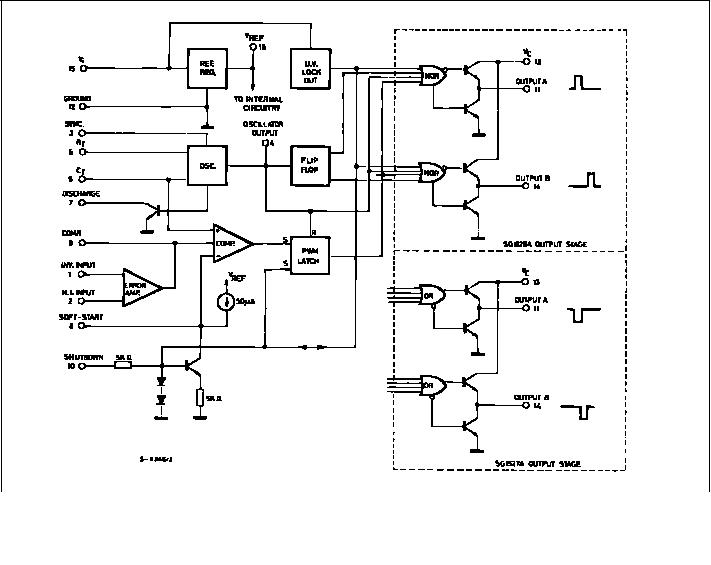
I have questions on SG3525. It says that the latch following the comparator will reset with each clock cycle. However, I do not understand how SG3525 can do that.
There is another question on the dead time. During this period, the outputs will be off. Again, I still do not know how SG3525 can do that. Wish someone can help me out.

https://www.ortodoxism.ro/datasheets/TelComSemiconductor/mXuwwxu.pdf
 

how to connnect an sg3525

hi,

83_1167607158.JPG


pin 15 ref out, basically 5V out

pin 6 & 5 for the oscillator input

if you give the freq from function generator then connect on the pin 3

then output latch toggle with the freq input from pin 3 or pin 5&6

but the output latch is also depend on the comparator input
 

sg3525+connect

Hello

My question are the following:

1.When does the latch reset and set ? At Ta or Tb

2.During the time period from Ta to Tb, which is the dead time, are outputs(PIN 11 and PIN14) off ?

I think outputs should be off simultaneously during the dead time according to the datasheet. However, I just do not get that.
3. What is the RS latch for here and how does it work?
 

Re: Questions on SG3525

yschuang said:
Hello

My question are the following:

1.When does the latch reset and set ? At Ta or Tb

2.During the time period from Ta to Tb, which is the dead time, are outputs(PIN 11 and PIN14) off ?

I think outputs should be off simultaneously during the dead time according to the datasheet. However, I just do not get that.
3. What is the RS latch for here and how does it work?


1........capacitor on pin 8 use to generate the delay b/w the pulses train on pin 14 and 11

2........it is calculated by the cap value at pin 8

3.........basically RS - latch input is connect to the comparator and output of the latch is connected with the output OR gate (use as the switch)

when the voltage on the inverting input is greater then noninverting input of the opamp so the RS-latch out put is high then OR gate is off

viseversa...... if not understand tell me
 

Re: Questions on SG3525

3.........basically RS - latch input is connect to the comparator and output of the latch is connected with the output OR gate (use as the switch)


So what kind of latch is it ? RS NAND Latch, D Flip-Flop, Clocked RS Latch
Thanks
 

Status
Not open for further replies.

Similar threads

Part and Inventory Search

Welcome to EDABoard.com

Sponsor

Back
Top