pseudockb
Member level 5
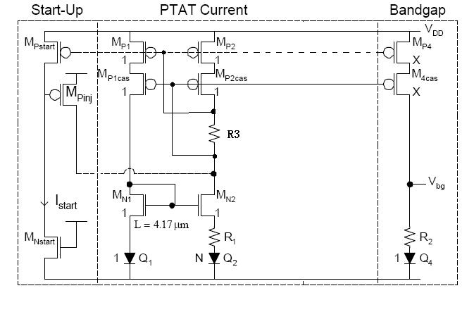
Cascode Bandgap
Hi all, I have some questions regarding the cascode bandgap.
1. Could someone please explain to me how the start-up circuit works? My understanding is that the NMOS acts as a pull-down resistor to pull the voltage at the gate of Mpinj to GND so as to inject a current into the bandgap core. How does the start-up circuit turn off? Or is it operating at all times? How does Mpstart come into play?
2. What is the reason of connecting Q3/Q5 at the bottom of cascode biasing transistors?
3. I can diode connect transistors MP2 so that I can remove the M3 transistors to save a branch of current. Any bad effect of this?
4. Intuitively speaking, the PSRR of this bandgap is a resistive devision between the output impedance of the cascode current mirror and the R2. I have heard that bandgap circuit utilizing an opamp clamping the at the top of Q1 and top of R1 can achieve a better PSRR compared to the cascode bandgap. Why is it so?
Thanks.