abcyin
Full Member level 4
Hi, all
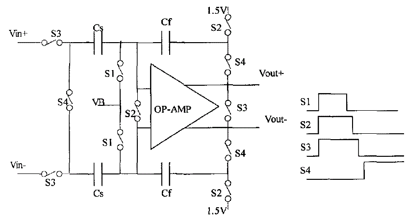
When I was trying to design a Sampling and hold circuit as shown in the following figure, I met a problem about the opamp in the circuit. The question is that, is that ok if there is no input DC voltage bias for the opamp in the hold period? When I was simulating the circuit, the output is ok as expected, but is the simulation really correct? or is there any potential danger for using this circuit?
Thanks in advance!