Ravinder487
Full Member level 3
- Joined
- Jul 9, 2010
- Messages
- 169
- Helped
- 0
- Reputation
- 0
- Reaction score
- 0
- Trophy points
- 1,296
- Location
- Bangalore, India
- Activity points
- 2,469
Hi all,
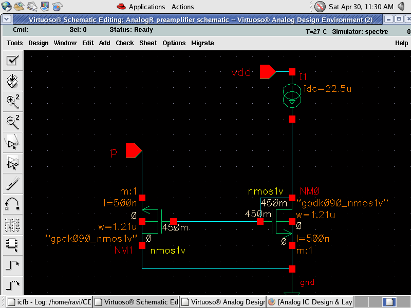
I want to mirror 22.5 uA current from reference current mirror(Diode connected transistor shown in image attached).Reference current mirror is biased at gm/id =7.With gm/id=7 VGS should be equal to 450mV, as VGS=VDS for diode connected load,node 'p'(pin p in schematic) should also be at 450mV so as both the transistors(NM0 and NM1) are perfectly matched.
If NM1 is used as tail current souce VDS of 450mV should be allocated to it which results in zero output swing for my circuit.