suria3
Full Member level 5
Hi,
I have a question. I'm working on a DC offset cancellation circuit in the feedback loop.
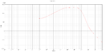
It it targeted for the bandwidth range of 500kHz. When, I plot the freq response of the bandpass
filter of the dc cancellation circuit, I'm seeing the freq response as per attached. The 3dB bandwidth on the f(low) is ~350khz
and f(high) is 3kHz. Then on the functionality side, I'm able to get the dc offset cancellation circuit to operate correctly, means
when I manually introduce DC mismatch at the input of the 1st stage, the dc mismatch is able to cancel out
at the last stage.
The question is, from the bandpass response, at ~0Hz freq, I'm seeing the gain in dB about 70dB. Isn't at the low freq operation,
the waveform suppose to show the DC gain number closer to 0dB or anything in the negative dB number as to attenuate the DC
signal? I understand at high freq the gain start to roll off due to capacitance effect, whereby on the low freq side, the dc gain
started from some steady DC value. So, in this case, should I assume the DC gain of 70dB is expected and I should not be
worried on the bandpass response as long the dc cancellation feedback loop is operating correctly, with meeting the f(low) and f(high).
Please help to explain on this.
Thanks
Suria
I have a question. I'm working on a DC offset cancellation circuit in the feedback loop.
It it targeted for the bandwidth range of 500kHz. When, I plot the freq response of the bandpass
filter of the dc cancellation circuit, I'm seeing the freq response as per attached. The 3dB bandwidth on the f(low) is ~350khz
and f(high) is 3kHz. Then on the functionality side, I'm able to get the dc offset cancellation circuit to operate correctly, means
when I manually introduce DC mismatch at the input of the 1st stage, the dc mismatch is able to cancel out
at the last stage.
The question is, from the bandpass response, at ~0Hz freq, I'm seeing the gain in dB about 70dB. Isn't at the low freq operation,
the waveform suppose to show the DC gain number closer to 0dB or anything in the negative dB number as to attenuate the DC
signal? I understand at high freq the gain start to roll off due to capacitance effect, whereby on the low freq side, the dc gain
started from some steady DC value. So, in this case, should I assume the DC gain of 70dB is expected and I should not be
worried on the bandpass response as long the dc cancellation feedback loop is operating correctly, with meeting the f(low) and f(high).
Please help to explain on this.
Thanks
Suria