Hawaslsh
Full Member level 3
- Joined
- Mar 13, 2015
- Messages
- 164
- Helped
- 5
- Reputation
- 10
- Reaction score
- 7
- Trophy points
- 1,298
- Location
- Washington DC, USA
- Activity points
- 3,422
Hello All,
I was looking through a few USBc parts for an edge mount PCB and i came across a connector that confused me and I thought I'd ask the community. The part in question is the UC-31PFFH-QF7001, I linked the data sheet i got from the company.

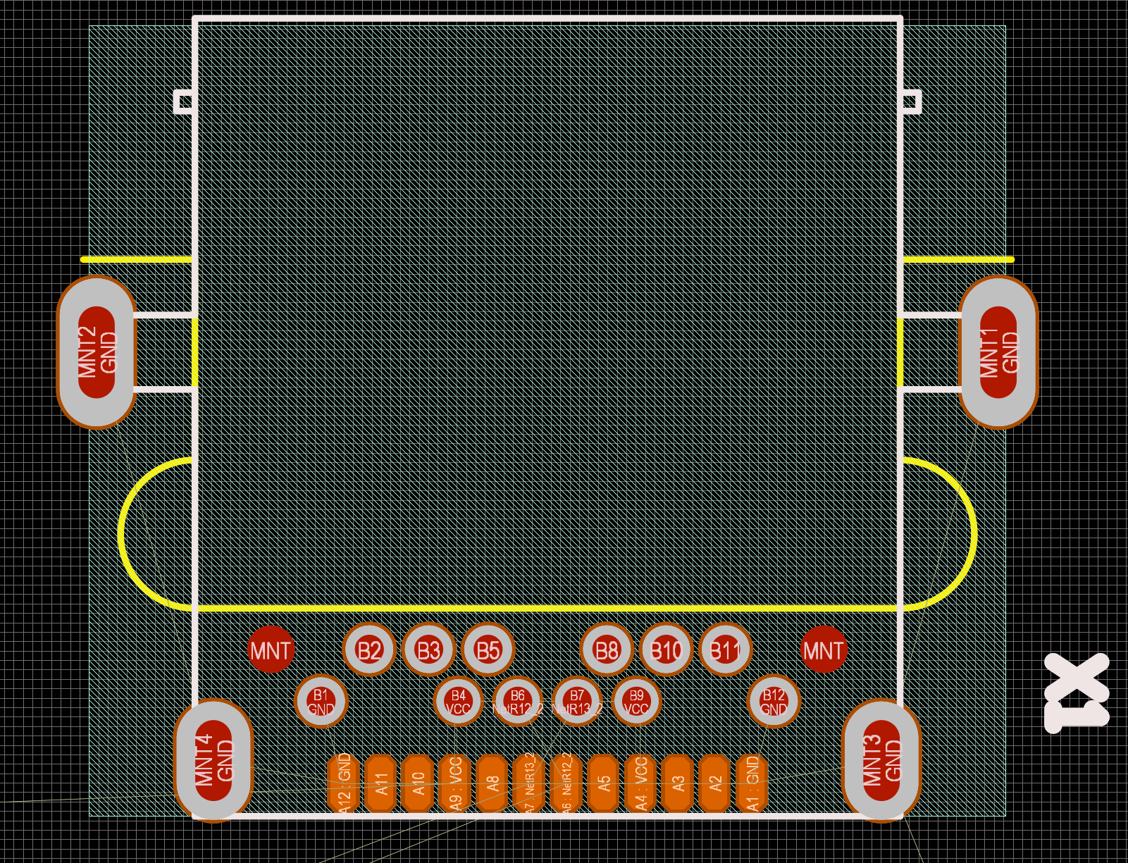
Above is the footprint and 3D model from the company. Each top side (orange) pad/net has a corresponding via associated with it. I can't tell from the drawing in the data sheet, are the pads and vias internally connected through the connector? For example is B6 (NetR12_2) internally connected to A6 (NetR12_2) and there is no need to route a trace connecting them? I suspect this is true for convivence of routing, but I wanted to ask instead of assuming.
Thanks in advance,
Sami
I was looking through a few USBc parts for an edge mount PCB and i came across a connector that confused me and I thought I'd ask the community. The part in question is the UC-31PFFH-QF7001, I linked the data sheet i got from the company.
Above is the footprint and 3D model from the company. Each top side (orange) pad/net has a corresponding via associated with it. I can't tell from the drawing in the data sheet, are the pads and vias internally connected through the connector? For example is B6 (NetR12_2) internally connected to A6 (NetR12_2) and there is no need to route a trace connecting them? I suspect this is true for convivence of routing, but I wanted to ask instead of assuming.
Thanks in advance,
Sami