naeemmaroof
Newbie level 4

- Joined
- May 11, 2006
- Messages
- 6
- Helped
- 0
- Reputation
- 0
- Reaction score
- 0
- Trophy points
- 1,281
- Activity points
- 1,331
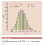
When we talk about 90nm process, what do we mean by this. Does it mean that minimum channel length (Ldrawn) is 90nm? or Ldrawn is 180nm? In attached image from a journal paper [1], author is referring to 90nm process, but has mentioned that L=46nm.
But previously we knew that according to lambda based rule, minimum channel length must be twice lambda. What is lambda in 90nm process? is it 45nm or it is 90nm? Do we still follow this rule? How author can make 46nm channel length in 90nm process?
Also, another question I have is that ... how do I find Leffetive? I know that it is Leff = Ldrawn - 2dL, but where to find dL ?
[P.S: There is no parameter named 'dl' or 'deltal' in 90nm process I have]
Ref:
[1] K. Bernstein et al., "High-performance CMOS variability
in the 65-nm regime and beyond", IBM J. RES. & DEV. VOL. 50 NO. 4/5 JULY/SEPTEMBER 2006
Regards,
Naeem

