Continue to Site

Welcome to EDAboard.com

Welcome to our site! EDAboard.com is an international Electronics Discussion Forum focused on EDA software, circuits, schematics, books, theory, papers, asic, pld, 8051, DSP, Network, RF, Analog Design, PCB, Service Manuals... and a whole lot more! To participate you need to register. Registration is free. Click here to register now.

Question about emitter graph

Status
Not open for further replies.

external

Newbie level 3
Joined
Jun 19, 2010
Messages
4
Helped
0
Reputation
0
Reaction score
0
Trophy points
1,281
Activity points
1,313
emitter-common doubts

hi

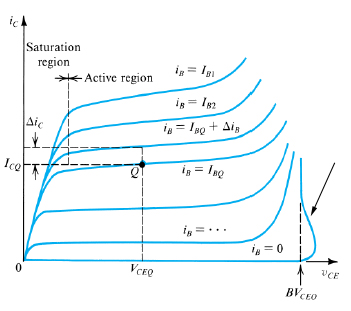
i don't have any clue on this graph. Why the line marked with the arrow has this "wave" line? It seems that this is not a function since we see that BVceo has over one value... Why this rupture happens? The "wave" line doesn't make sense!

what is the meaning of the Q point?? Maybe it means that is a biasing point where we can have the signal amplified without distortion?

I did not understand the differences between beta for DC and AC beta. Please someone can explain it to me? Thank you.

Look at the image filename... why there is no signal component between colector and the emitter????

please, help in this.


52_1276960999.jpg
 

Re: emitter-common doubts

The marked region above Vce0 is designating avalanche breakdown. You shouldn't operate a transistor in this region under regular conditions.

Q is an abitrary bias point. In my opinion, it doesn't make much sense to discuss it without a specific application circuit, particularly a load impedance. Most text books are adding a load line to the Vce-Ic diagram.

There are different terms for large signal (DC) and small signal (AC) current gain in use. Following your nomenclature, βDC is simply the quotient IC/IB, βAC is the gradient dIC/dIB.

I don't know which image filename you're talking about...
 

Re: emitter-common doubts

here the "image" filename. Well the edaboard gave a different name. :)

32_1276960999.jpg
 

Re: emitter-common doubts

No filename is shown for embedded images..

why there is no signal component between colector and the emitter????

Do four question marks suggest a question well justified by an uncleat text? You should read the text exactly. It's simply about the definition of a term. It says, that the current gain has to be measured with constant Vce. If you allow Vce to change with Ic, the transistor output resistance must be considered in the calculation, if you don't, you get a "pure" current gain.
 

Status
Not open for further replies.

Similar threads

Part and Inventory Search

Welcome to EDABoard.com

Sponsor

Back
Top