Continue to Site

Welcome to EDAboard.com

Welcome to our site! EDAboard.com is an international Electronics Discussion Forum focused on EDA software, circuits, schematics, books, theory, papers, asic, pld, 8051, DSP, Network, RF, Analog Design, PCB, Service Manuals... and a whole lot more! To participate you need to register. Registration is free. Click here to register now.

quesetions on the topology of push-pull converter

Status
Not open for further replies.

jonny200903

Newbie level 3
Joined
Jun 10, 2016
Messages
3
Helped
0
Reputation
0
Reaction score
0
Trophy points
1
Activity points
27
Hi Sir,

In the topology of push-pull, when the swith is off, there is a spike created by the leakage inductance at primary. My question is which path to absorb this spike in standard push-pull circuit.
Another question is: when one of primary switch is on, there is magnetizing current due to the magnetization inductance of the primary, how to reset it to avoid the magnetic saturation. Thanks!
 

Presume "push-pull" refers to transformer push-pull (half- or full-bridge is push-pull as well).

Usually leakage inductance spikes are absorbed by dissipative snubbers, e.g. RCD or diode + Z-diode combination. Use interleaved primary windings to make the leakage inductance between both windings low.

Magnetizing current is AC current and doesn't need dedicated reset. A possible saturation problem arises with asymmetric duty cycle or circuit. With less than 50 percent duty cycle, the asymmetric magnetization should still reset during free wheeling phase. A small air gap can help in this regard. Or use primary current measurement and active flux balancing.
 

A standard push pull relies on very good coupling between the primary windings, so that when the fet switches off (with magnetising and load current) in its winding, the leakage inductance is minimal and the energy goes to the other winding (the wrong way thru the other mosfet) and into the local supply decoupling cap, there are variations on the push pull that deal with this turn off energy on other ways, requiring at least one extra cap, but for the standard ckt good coupling and some small amount of snubbing on fts and o/p diodes will fit the bill.
 

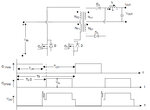
Added the circuit of push-pull as below.
When the switch of Q1 is off, there is a spike at the non-dot of Np1. Could body diode of Q2 creat a path to flow this leakage energy to the input capacitor(the capacitor paralleled with input voltage is not showed in the circuit)? If so, why is it?
QQ截图20160628155625.jpg
 

In the real world you need a good quality cap from the transformer CT to the 0v by the fet sources, this is the difference between theory (books, web notes, simulation etc) and practical knowledge...
 

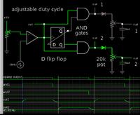
This switching method might be of interest. Mosfet turn-off is less abrupt. High voltage spikes might be reduced.


Adjust values to shape the waveforms as desired.

The mosfets spend some time midway between full-Off and full-On. This is liable to cause mosfets to heat up. It should be considered an experimental method.
 

Status
Not open for further replies.

Part and Inventory Search

Welcome to EDABoard.com

Sponsor

Back
Top