Continue to Site

Welcome to EDAboard.com

Welcome to our site! EDAboard.com is an international Electronics Discussion Forum focused on EDA software, circuits, schematics, books, theory, papers, asic, pld, 8051, DSP, Network, RF, Analog Design, PCB, Service Manuals... and a whole lot more! To participate you need to register. Registration is free. Click here to register now.

Quartus Prime Lite 18.1 async fifo ip question

Status
Not open for further replies.

MagicToad

Newbie
Joined
Jun 8, 2022
Messages
2
Helped
0
Reputation
0
Reaction score
0
Trophy points
1
Activity points
22
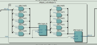
I currently use the quartus, the verison is described in title. And I instantiated an async fifo ip, synthesized it. Then I open the RTL viewer, in a module(its function is to sync the write gray code ptr to read side) I have seen a weird logic combination. In my thought this module should simply have two regs which are used for different clock syncing, but it has each bit of gray_coded ptr through an and gate(the gate's other input is a constant 1) then to a reg then through and gates finally through regs and output to read side. It also did for read to write side.
I did not know why it does that, anyone has any idea?
 

Attachments

  • async_fifo_ss.png
    async_fifo_ss.png
    20.2 KB · Views: 158

You can't clock domain cross a signal with multiple bits and get guaranteed valid data in the register in the new clock domain.

e.g. 01111 +1 => 10000, the carry is propagated and the routing delays are non-zero.

If you try and capture this changing value on a new clock domain you could potentially sample any combination of bits, that have the old value or the new value.

grey coding only allows 1 bit change at a time, so sampling it in a new clock domain means you are only syncrhonizing 1 bit instead of 5-bits in the example above.
Well, I think you didn't get my question. I know the purpose of using gray code in asyc fifo. In the pic, the input to this module are already the gray code format. My question is why add and gate before regs?
 

It makes little sense to pick a small snippet out of a RTL circuit and ask why it looks like it does. Often RTL details represent redundant logic or unused features of the core. Physically, the gates are placed inside LEs and don't consume extra logic resources.

To understand how the RTL circuit is formed, you have to look into the IP HDL sources.
 

I think it is only a "dummy" representation for a straight "pass-thru", where the output from the LUT is the same as the input. As already mentioned, the LUT and the register come together, so there is no "cost" for the shown logic gate.
 

It seems those are for initializing the registers.
Definitely, those are not for initialization purposes.

They are there to introduce combinational delay to allow you to clock in the old data that was there at the D inputs of the flip-flops.
 

Status
Not open for further replies.

Part and Inventory Search

Welcome to EDABoard.com

Sponsor

Back
Top