Continue to Site

Welcome to EDAboard.com

Welcome to our site! EDAboard.com is an international Electronics Discussion Forum focused on EDA software, circuits, schematics, books, theory, papers, asic, pld, 8051, DSP, Network, RF, Analog Design, PCB, Service Manuals... and a whole lot more! To participate you need to register. Registration is free. Click here to register now.

Push-pull output switches OFF momentarily after switching ON

Status
Not open for further replies.

mrinalmani

Advanced Member level 1
Joined
Oct 7, 2011
Messages
463
Helped
60
Reputation
121
Reaction score
58
Trophy points
1,318
Location
Delhi, India
Activity points
5,285
Hi
A 3.3V PWM input is stepped up to 12V using a BJT. The BJT has a speed up capacitor of 50pF. The output from the BJT is fed to an inverted push-pull stage. (Inverted as in the P MOSFET is at the bottom and N at the top)
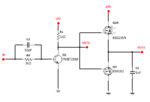
Capture.PNG

The problem is that soon after the BJT switches ON, it immediately switches OFF for a few nano seconds and then switches ON again.
1. When the speed up capacitor is removed, there is no such problem.
2. Or when load capacitor is reduced to a small value, again the problem dissapears.
See the waveform of switching.
Black: Out1
Red: Out2
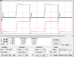
Capture1.PNG

Why is the BJT turning off momentarily?

Thank you!
 

Hi,

is this a real circuit measurement or a simulation.

I expect: real circuit. Then it might not switch off it´s just a measurement problem. --> Long cable, not suitable scope probe, wrong GND connection...

Klaus
 

Unfortunately this is a simulation.
And the turn-off is probably not due to stray inductance because adding nearly 5nH inductance in series with the speed up capacitor does not change the result.

However adding a 100 Ohm resistor in series with the BJT output and totem pole input eliminates this problem.
 

Why is the BJT turning off momentarily?

This is due hard turn off; You can see the slope in the rise part of the square wave but there is very large slope in the turn-off part.

You need a small resistance in series with the gate charging and discharging.

You also need a bypass capacitor in parallel with R1.

What is wrong with hard turn-on and turn-off? The very large di/dt involved can couple with parasitic capacitances/ inductances and cause this spike. See https://en.wikipedia.org/wiki/Gibbs_phenomenon

The circuit is tending to oscillate because there is no bandwidth limitation.
 

What is wrong with hard turn-on and turn-off? The very large di/dt involved can couple with parasitic capacitances/ inductances and cause this spike.
Sounds rather vague and highly speculative. You're not actually saying how the waveform could be generated. There's no parasitic inductance present in simulation unless you are using package models or adding dedicated circuit inductances.

On the other hand, if it's a simulation, you can answer the question yourself by looking at device currents.
 

Sounds rather vague and highly speculative..

I admit. I really do not know how these simulations work (vaguely, yes; details, not) and can only speculate on some aspects.

1. If you add a small capacitor in parallel with R1, the rise time will increase but the fall time will not change. The gate capacitor must be part of the model and it gets charged via R1 and discharges via the transistor (which is also part of the model: must be very small). The square wave is clearly not symmetrical.

2. If you put a small resistor in series with the gate charging (and discharging) the square wave will be almost symmetrical. The ringing will almost disappear. I say almost because...

3. You are right when you say that there are no parasitic inductance (or perhaps capacitance) used in the simulations- right but they are present not explicitly but virtually.

They are present 'virtually' because all these simulations are carried out in discrete points space. They imply a cut-off in bandwidth (Nyquist theorem). This is really not a limitation but a feature because all real physical devices have finite bandwidth response functions. The phase shifts produce this ringing pattern.

When I say very large di/dt are involved, I mean that there are too few points to integrate numerically in the fast rising part. But putting too many points is useless too because the increase in bandwidth will be consumed by the low pass filters formed by the circuit elements. In that sense this simulation is realistic and will be seen in actual experiments. I do not know whether I am clear enough.

By the way, I request mrinalmani to try the same simulation with (i) a 0.1 uF cap in parallel with R1 and (ii) 0.1 uF cap in parallel with R1 AND 10 ohm resistance in series with the gate.
 

Status
Not open for further replies.

Similar threads

Part and Inventory Search

Welcome to EDABoard.com

Sponsor

Back
Top