Continue to Site

Welcome to EDAboard.com

Welcome to our site! EDAboard.com is an international Electronics Discussion Forum focused on EDA software, circuits, schematics, books, theory, papers, asic, pld, 8051, DSP, Network, RF, Analog Design, PCB, Service Manuals... and a whole lot more! To participate you need to register. Registration is free. Click here to register now.

Pure sinewave SPWM inverter

Status
Not open for further replies.

Kryptone

Member level 3
Member level 3
Joined
Mar 14, 2014
Messages
64
Helped
2
Reputation
4
Reaction score
2
Trophy points
8
Visit site
Activity points
552
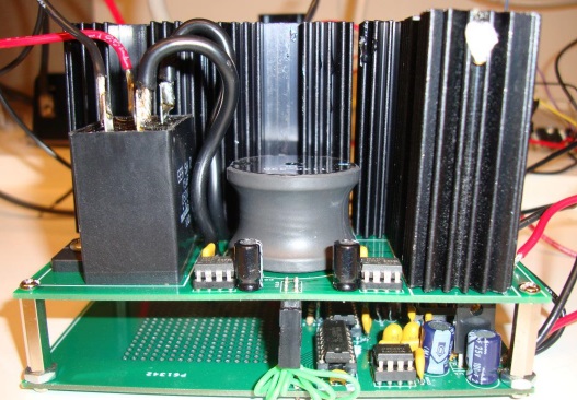
I am designing a SMPS inverter I need 110VAC , 50Hz output with 12V input from power supply. I built my dc-dc converter using a ETD34 ferrite core with windings 3 + 3 turns on the primary and about 80 turns on the secondary in order to get 180 Vdc after feedback.

The dc-dc converter worked and now I am on to the SPWM section where I am using the ATmega16 to generate the SPWM signals . When I simulate the code in Proteus it works giving me my 50 Hz fundamental frequency and 16kHz switching frequency but when I connect the pins of the MCU to the full bridge inverter I can see the switching of the MOSFETs but I get zero voltage at the outputs but when I connect the AC voltmeter in Proteus across the LC filter to ground I get about 60 VAC which decreases after a while from the 180 VDC dc rail of the full bridge inverter. WHat could be wrong?


From the snipped image of the circuit shows that Q1 and Q3 turn on while Q2 and Q4 are off for 8ms and then vice-versa
SPWM capture.PNG


Please I need help!!!!!!!!!!
 

A gate drive circuit is required between mcu-pins and output-FETs. Two IR2110 ICs can do this job.
 
A gate drive circuit is required between mcu-pins and output-FETs. Two IR2110 ICs can do this job.


Ok cool so if I were to parallel an extra MOSFET on each leg (high and low side)ie. 4 more, could I still use two IR2110 to drive them. Also what filter LC values could I use to get rid of the switching frequency and only get the fundamental frequency of 50Hz?

I did some reading that the inductor requires a min load for it to work efficiently please clarify this for me and help me design an appropriate filter that will work.
Circuit Diagrams would be welcomed.
 

Kryptone said:
Ok cool so if I were to parallel an extra MOSFET on each leg (high and low side)ie. 4 more, could I still use two IR2110 to drive them. Also what filter LC values could I use to get rid of the switching frequency and only get the fundamental frequency of 50Hz?
you must use the high low side driver IC (like IR2110) as suggested by ALERTLINKS.
In the present scenario , the high side mosfet are not getting ON , because in order to fully turn on the power mosfet the Vgs should be greater than 8V , suppose the DC link to the H-Bridge is 180V , as the high side mosfet will turn On , the source will be at 180V with respect to ground, so in order to turn the mosfet ON , you have to apply atleast (180+8)V to the gate wrt ground so that the VGS should be atleast 8V , this can be done using bootstrap capacitor incorporated in IR2110, or pulse transformer.
 

    V

    Points: 2
    Helpful Answer Positive Rating
Q1 and Q3 turn on while Q2 and Q4 are off for 8ms and then vice-versa
If Q1 and Q3 both conduct at same time, it will shorten the DC-bus and FETs will be destroyed. Upper switches receive 16 KHz pulses and lower switches receive 50Hz or 60Hz pulses in pure sine wave modulation. So the input to gates should be like this that when Q3 is switched on for 8mS then gate of Q2 receive 16KHz modulation pulses. When Q4 is on for 8mS, Qi gets the 16KHz pulses. In this wasy current flows through the load in alternate directions and hence AC-output is generated.

https://www.edaboard.com/threads/233717/
https://www.edaboard.com/threads/250505/
 

    V

    Points: 2
    Helpful Answer Positive Rating
Hello ALERTLINKS,

can you help me design a suitable LC filter to get a pure sine wave at the output and rid of the switching frequency and pass the fundamental frequency of 50 or 60 Hz? I tried various combinations of Land C and still not getting a pure sine wave in Proteus. Also, does the inductor require a min load in order to work properly? I read this some where.

Please help!!!!
 

Kryptone said:
can you help me design a suitable LC filter to get a pure sine wave at the output and rid of the switching frequency and pass the fundamental frequency of 50 or 60 Hz? I tried various combinations of Land C and still not getting a pure sine wave in Proteus. Also, does the inductor require a min load in order to work properly? I read this some where
For your simulations purpose use resistor in place of inductor because using LC filter in proteus results in error. Proteus does not simulate L as desired.so i will suggest that use RC filter for your simulations purpose in proteus.
And for practical circuit use LC filter.
Now how to select L?
L should be selected in such a way that the impedence offered by the L at fundamental frequency is 2% to 3% of charecterstics impedence of your inverter.
Now after getting the value of L. You can easily get C using relation F=1/2*pi*root(L*C).

Now come to the output minimum load; the min load depends on the scheme that u are using . if u r using asynchronous spwm scheme :u wud be required to put some minimum load at the output to see the sine wave in oscilloscope .so i suggest to put some mimimum load at the output say(3 watts).
 

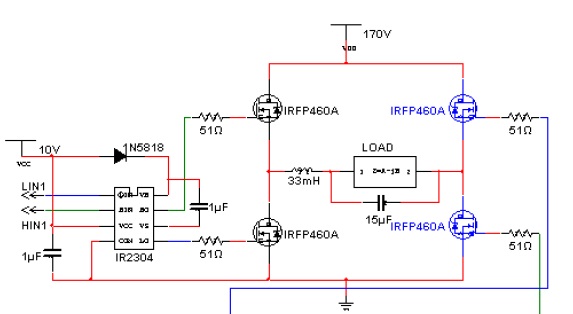
In an application note for a 300-watts inverter for 110V-AC output it uses 33mH inductor and 15uF capacitor.

2555929700_1396262641.jpg


2960709700_1396264358.jpg
 

Mr Bawa,

Not quite understanding the asynchronous spwm scheme. Could you provide me with an example are so. for the spwm section I am using the MCU connected to 2 MOSFET drivers and then to the full bridge inverter. I am using switching frequency of 16 KHz and 50 or 60 Hz fundamental frequency. Also, what could I use for the min load could a say 1 ohm 3W resistor be used?

Also, if I parallel MOsfets in the bridge can I still use just 2 MOSFET drivers?

- - - Updated - - -

Mr. ALERTLINKS,

the load in the circuit is that the min load soldered in the circuit or is it a load connected to the circuit? If thats the case I would have to leave a space for it in my PCB. I also read somewhere about placing the load in series with the inductor and in parallel with the capacitor. I have also seen them use a thermal resistor in series with the cap as a min load.
 

300W is maximum external load. You can see it is in series with the inductor. Capacitor is connected parallel to the load. In most cases, inverter is operated with enough load. If waveform distorts at no load, who cares. This problem should be dealt in the end.
 

300W is maximum external load. You can see it is in series with the inductor. Capacitor is connected parallel to the load. In most cases, inverter is operated with enough load. If waveform distorts at no load, who cares. This problem should be dealt in the end.


Mr. ALERTLINKS,

If I parallel MOsfets in the bridge ie. 4 high side 4 low side can I still use just 2 MOSFET drivers to drive them? I want to achieve more power by paralleling them.
 

Kryptone said:
Not quite understanding the asynchronous spwm scheme. Could you provide me with an example are so
i presumed that you are using asynchronous scheme , this scheme basically incorporate BIPOLAR SPWM or modified BIPOLAR SPWM. In this driving scheme the one mosfet is driven by a SPWM signal while the other diagonally opposite mosfet is driven by the complimentary of that SPWM. May be in your case , you are firing the gate of one mosfet with 16KHz SPWM signal , while keeping the diagonally opposite side mosfet fully turn ON for entire 8 millisecond . These are the example of 2 quadrant operations.
Synchronous scheme like UNIPOLAR SPWM is quite better than BIPOLAR one because , if you are using 16KHz carrier frequency , the output load will see double of that frequency (32KHz), so the size of filter reduces , also this scheme is four quadrant operation , and the stress on the BODY DIODE of the mposfet is quite low.
**broken link removed**

Kryptone said:
Also, what could I use for the min load could a say 1 ohm 3W resistor be used?
i have said that it should be somewhat around 3 watt , and your inverter's output voltage is 110V so the if you use the relation P=square(V)/R. u"ll get R= 4033 ohms , not 1 ohm, and don't use 1ohm resistor , it will draw a huge current ,which will overshoot your inverter's maximum current capability. you just simply use a 5 watt bulb for your testing purpose.
 

Mr. Bawa,

should this min load be placed in series with the inductor and in parallel with the capacitor as shown by Mr. ALERTLINKS?

If so then the external load would then be placed in parallel to the min load or cap?
 
Last edited:

Yes alertlinks is right. The min load should be placed in parallel to capacitor.
Its basically a low pass lc filter so the load must be connected parallel to capacitor only.
 

Hello Mr. ALERTLINKS and Mr. BawA,
for my MCU generating the SPWM signal do I have to use an external crystal oscillator or can I use the internal one? most stuff I see use the external crystal on the MCU.

Also, do I need a min load to get a 110 VAC reading on the multimeter. I tested my circuit and when I put a LED across the drain of a low side MOSFET it lights up but not getting a reading on the multimeter at the ouput and I used 2 MOSFEt drivers and a 180 Vdc bus.

Please Help!!!!!!!!
 

In an application note for a 300-watts inverter for 110V-AC output it uses 33mH inductor and 15uF capacitor.

2555929700_1396262641.jpg


2960709700_1396264358.jpg


ALERTLINKS,

When I connect my dc-dc converter to the drains of my full bridge inverter my ferrite core tranformer begins to make a sound and then after a little while I see smoke coming from it. What could be the problem? I was wondering if it could be the LC filter at the output of the dc-dc converter maybe it needs to filter better to smooth the dc voltage to the inverter? not sure though.

The led that I placed across the drain of one of the low side Mosfets lights up but I hear the noise from the transformer and then I see smoke from it then I switch off the circuit otherwise when not connected to the full-bridge inverter it works fine giving 180Vdc with no sound from the Ferrite core transfromer.

Please help!!!!
 

if your mcu supports internal oscillator module with PLL, you can use it , otherwise use external one .

Kryptone said:
Also, do I need a min load to get a 110 VAC reading on the multimeter. I tested my circuit and when I put a LED across the drain of a low side MOSFET it lights up but not getting a reading on the multimeter at the ouput and I used 2 MOSFEt drivers and a 180 Vdc bus.
increase your load , led is not a sufficient minimum load , you can use 5w bulb for testing purpose , and it should be connected parallel to capacitor of LC filter.
 

Mr. BaWa,

When I connect my dc-dc converter to the drains of my full bridge inverter my ferrite core tranformer begins to make a sound and then after a little while I see smoke coming from it. What could be the problem? I was wondering if it could be the LC filter at the output of the dc-dc converter maybe it needs to filter better to smooth the dc voltage to the inverter? not sure though.

The led that I placed across the drain of one of the low side Mosfets to ground lights up but I hear the noise from the transformer and then I see smoke from it then I switch off the circuit otherwise when not connected to the full-bridge inverter it works fine giving 180Vdc with no sound from the Ferrite core transfromer.
 

To rectify the problem that you are facing , just follow the steps below.
1) connect a 100 watt bulb (filament type )as a resistive load to the DC DC converter stage , and check the output voltage ,don't put any inductive or capacitive load to DC DC stage output.
if bulb glows , with no smoke in ferrite core, it will imply that your DC DC stage is perfect .

2) connect your H-Bridge to a low voltage DC source (say 12V), and see the output waveform in oscilloscope. it should be a sine wave , as i already mentioned that you are using modified version of bipolar SPWM , so ensure that you are using some minimul load connected parallel to the capacitor.

3) make sure that you have provided a proper dead time between signals.

4) what is the value of bulk capacitor that you are using at the DC link voltage to the H-Bridge? and which type of capacitor is it?

5) to test your H-bridge at high voltage DC bus , connect a 100 watt bulb in series with H-Bridge . it will protect your mosfets from burning.
 

Mr. BaWa,

Here is the schematic for my DC-dc converter


I however used 4 Mosfets ie. I paralleled one with the high side Mosfet and the other with the lowside Mosfet
 

Status
Not open for further replies.

Similar threads

Part and Inventory Search

Welcome to EDABoard.com

Sponsor

Back
Top