Continue to Site

Welcome to EDAboard.com

Welcome to our site! EDAboard.com is an international Electronics Discussion Forum focused on EDA software, circuits, schematics, books, theory, papers, asic, pld, 8051, DSP, Network, RF, Analog Design, PCB, Service Manuals... and a whole lot more! To participate you need to register. Registration is free. Click here to register now.

[SOLVED] Pure sinewave inverter with toroidal transformer

Status
Not open for further replies.
I'm using an unipolar scheme, indeed. One low-side switch is closed at any time but still the floating point of the other bridge leg has very big voltage oscillations (over DC-link and under GND levels) thus I prefer to put snubbers across every switch. And, as a feedback, all snubber resistors (high-side and low-side) are getting warm almost equally.

At first, I was just using big TVS diodes alone (3 x 5kW rated) across every switch but they were getting hot very fast. The DC-link voltage was 24V (it will be 48V at the end) and the TVS diodes were 75V rated (the MOSFETs are 200V rated though).

Anyway, the switching noise is highly disturbing the high-side bootstrap supplies thus I won't run any further test until I'll finish those separate/isolated power supplies for every MOSFET driver.
 

I'm using an unipolar scheme, indeed. One low-side switch is closed at any time but still the floating point of the other bridge leg has very big voltage oscillations (over DC-link and under GND levels).

The fact that the MOSFETs are clamping voltage levels beyond the rails suggests that you have a lot of parasitic circuit inductance implemented, and/or gate signals faster than suitable.
 

    V

    Points: 2
    Helpful Answer Positive Rating
Thanks for the reply, I'll be going this in a month or so myself. Technically, you only need 2 isolated power supplies and one ground referenced non isolated supply - am I correct? Are you going to do 4 isolated supplies because its just as easy as doing the 2?
 

The fact that the MOSFETs are clamping voltage levels beyond the rails suggests that you have a lot of parasitic circuit inductance implemented, and/or gate signals faster than suitable.

Thanks, @FvM! I've already increased the gate resistors ten times (4.7R > 47R) and I removed the reverse forwarding diode across those gate resistors, too (to slow down the turn off process).

I'm using 4 paralleled MOSFETs for each switch, mounted on the same heatsink. From that PCB, I'm running a thick wire (16mm / 10cm long) toward DC-link and toward the transformer primary. Do you think the parasitic inductance of such a wire could be too high? Do I have to use flat copper bars or something, instead of those thick wires? Could you recommend a solution for a lower parasitic inductance?

The PWM frequency is 6.4kHz but there are higher armonics (the sPWM modulated duty cycle could be as low as 2-3% around the zero crossing point).

Technically, you only need 2 isolated power supplies and one ground referenced non isolated supply - am I correct? Are you going to do 4 isolated supplies because its just as easy as doing the 2?

@bitsfromadish:

Yes, 3 isolated power supplies should be enough but to eliminate any interference (during every half sine wave, while one low-side MOSFET is always ON the other one it's hard switched) I'm going to use separate power supplies for every driver. Moreover, I'm going to generate a separate (isolated) power supply for uC, too (while the inverter is running, the USB communication with the uC is sometimes lost). I'm already using optocouplers between the uC and the MOSFET drivers but the uC power supply is derrived from the DC-link and it's quite noisy while the inverter is running.
 

Still having hard time trying to remove the switching spikes/ringing across the MOSFETs (even with small loads - an 100W incandescent bulb).

I've redesigned the whole power board (the drivers are next to the MOSFETs, I'm using thick copper busbars instead of wires) but still can't figure out how to "cover up" that 150ns time gap (the MOSFET built-in diode recovery time) during which the switching node is just floating.

I've tried to use some RC snubbers (200nF/47ohm) but the resistors (3W rated) are getting hot pretty quick. I also have three 5kW TVS diodes (110V) across every switch and they are getting warm/hot, too.

if you use unipolar modulation it means you only need snubbers and or high speed diodes on the high speed switching quadrants of the bridge.

You were right, the upper switches snubbers/TVS diodes seem more affected. In theory (at least), the load current is zero when the low-side (active) MOSFET is turning off thus there's no need for any snubber here.

By using an unipolar scheme, one leg of the load (transformer) is tied up to ground while the other leg switches are driven by complementary PWM signals.

Anyway.. maybe I should recalculate those high-side snubbers?

Thanks in advance for any suggestion.
 

Does anyone know how to derate a TVS diode current carrying capability for a non-standard (transient) pulse?

The datasheet only mention the 10x1000us test waveform but I want to use them as "level two" snubbers across every H-bridge MOSFET thus the pulse period is much smaller (150us). Anyway, the deadtime (during which the TVS is active) is about 1.5us thus it could still follow the specifications (0.01% repetition rate).

Moreover, could them be used as freewheeling/clamping diodes, by any chance? They have a "Peak Forward Surge Current, 8.3ms Single Half Sine Wave Unidirectional Only" current of 400A. How to translate that?

This is the LittelFuse datasheet: https://www.littelfuse.com/~/media/electronics/datasheets/tvs_diodes/littelfuse_tvs_diode_5kp_datasheet.pdf.pdf
 

It really all comes down to heat and allowable temperature rise for sustained operation.

While they can clamp hundreds of amps for a few microseconds, they can only do it once, and then need a long cool down period before you can hit it like that again.

If it is sinking energy every cycle at 6.4 Khz, the physical size might realistically limit the continuous power dissipation to perhaps less than one watt.
Its not what they are really designed to do.
But if it does not burn itself up, it should certainly do the job.

Just putting your finger on it should tell you.
 

    V

    Points: 2
    Helpful Answer Positive Rating
Thanks, Tony! The TVS are rated around 8W (they are quite bulky). That's why I've used 3 of them in parallel across every switch (and I could further increase their number).

They are getting quite warm right now but that's because the RCD snubbers aren't doing their jobs yet.

I'm going to try to increase the capacitor value. I hope the voltage spikes will be attenuated enough to not reach the TVS breakdown voltage anymore.

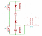
There are two RCD configurations:

DualSnubberCircuit.gif

I know that's a pretty common design for flyback converters but I wonder what's the best suited for my situation (the high-side switch).

- - - Updated - - -

In the first case (the top RCD topology in the image above), the capacitor is discharging through resistor only. In the second case, the capacitor is discharging through resistor and MOSFET.

Also, in the first topology, the current is flowing through resistor in both capacitor charging and discharging stages. So, what could be the most suitable?

- - - Updated - - -

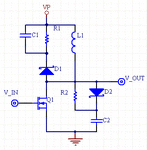
I came up to this configuration:

snubbers.gif

While the high-side MOSFET is in ON state, both capacitors are discharged.

When the high-side MOSFET is turning off, the middle node is driven bellow ground by the energy stored in the transformer leakage inductance thus both diodes are forward biased and both capacitors begin to charge, slowing down the voltage ramp across high-side MOSFET.

Any doubts about it?
 

The middle node can never go below the negative dc rail voltage at each individual mosfet because if the inherent source drain diode.
likewise the upper mosfet will clamp any positive load transients to the positive rail right at each mosfet.

Probing the circuit, you may see horrendous voltage spikes, but they cannot really be there, the diodes in each individulal mosfet guarantee it cannot really happen.

As you already know, the voltages you are seeing are generated by parasitic inductance, and especially transformer leakage inductance, and look nasty, but are not really of any threat to the mosfets as each protects itself individually with its own internal diode.

As mosfets do not suffer from second breakdown (as other switching devices do), the safe operating area for full load inductive turn off extends right out to the devices full voltage and current ratings. So load shaping turn off snubbers are not needed.

The fact that the system is still working and not already a blown up charred mass, suggests it is not entirely unhappy with the situation.
 

The MOSFET body diodes are not very fast (recovery time: over 150ns) thus during this time there's no clamping action.

Like I said before, the 110V TVS diodes placed across every MOSFET D-S were getting very hot, which means they were clamping hard an over 150V voltage spikes.

The actual (testing) DC-Link voltage is 24V thus the switching node went bellow GND with more than 100V right after the high-side MOSFET was turned off.

After implementing the above snubber configuration (and after increasing the capacitors values) the TVS diodes are staying cool (the transient voltage spikes were drastically reduced).

The next action will be to put some external high power Schotky diodes across every MOSFET for early clamping.
 

The shottky diode idea is the better way to go.
Solder one directly across every mosfet with minimum lead length.
 

Generally speaking, if a bridge converter needs snubbers, particularly snubbers with considerable power rating, there's something wrong with the converter design. That's because currents are commutated between low and high side switch, so layout inductance, transistor bond wire + package inductance and bus capacitor ESL are the only energy storing and possibly resonating circuit inductors.

A problem might be brought up by allowing current flow through the substrate diodes in a not fully synchronous switching scheme. In MOSFET bridge converter, the output node shouldn't be tristated for more than a few 10 nanoseconds, so that you get at worst part of the output current flowing through the substrate diodes.
 

    V

    Points: 2
    Helpful Answer Positive Rating
A problem might be brought up by allowing current flow through the substrate diodes in a not fully synchronous switching scheme. In MOSFET bridge converter, the output node shouldn't be tristated for more than a few 10 nanoseconds, so that you get at worst part of the output current flowing through the substrate diodes.

I made an erroneus statement in the previous post about the body diode recovery time as being the main limitation. Actually, the forward turn-on time is of the main concern when we're talking about voltage clamping and (reading from the IRFP4668 datasheet) that turn-on time is negligible. Then I really don't understand why there is such a big time gap during which the output node is floating. By the way, the deadtime is around 1.5us.

I have to mention that the MOSFETs stay cool all the time so there's no sign of stress caused by the substrate diode conduction.

Generally speaking, if a bridge converter needs snubbers, particularly snubbers with considerable power rating, there's something wrong with the converter design.

Although you're right, I've read some literature lately about snubbers being a must-to in high power designs (like welding inverters and such).

Regarding the converter design, I'm using thick (6mm * 30mm) copper flat bars as DC-link, GND and output rails. The parasitic inductances are very small in my opinion. Anyway, the snubbers/TVS diodes are placed right across MOSFETs.

- - - Updated - - -

That's because currents are commutated between low and high side switch, so layout inductance, transistor bond wire + package inductance and bus capacitor ESL are the only energy storing and possibly resonating circuit inductors.

By the way, when the high-side switch is turning off, all the energy stored in the transformer leakage inductance should be discharged (shunted) through the low-side switch freewheeling diode.

That means the DC-link decoupling capacitors have no contribution in this situation. Am I wrong?
 

Dead time is still needed, because current rise and current fall times are finite, and so are the respective gate delays involved.

So you always need to give turn off a head start, before turning on the opposite mosfet, to minimize or eliminate the possibility of cross conduction current spikes.

Dead time is a bit like like sleeping on the job.

If your whiz bang gizmo is rattling along at 100 Khz, 1uS is about ten percent of the cycle time when nothing worthwhile is happening.

At 6.4 Khz, 1.5uS is a rather small proportion of 156uS cycle time, so its nothing to be concerned about.
Its better to allow the system a bit of slack rather than run into the evils of cross conduction even if only very slight.

You can never really tristate a system with an inductive load, well you can, but the voltage slams up or down into the drain source diodes pretty smartly anyway regardless of dead time.
Its just that during dead time no useful power is transferred.
 

Although you're right, I've read some literature lately about snubbers being a must-to in high power designs (like welding inverters and such).
Just can tell that the MOSFET and IGBT inverters I'm working with (up to several 10 kW per bridge leg) don't use snubbers. But there may be different desigms.

By the way, when the high-side switch is turning off, all the energy stored in the transformer leakage inductance should be discharged (shunted) through the low-side switch freewheeling diode.

That means the DC-link decoupling capacitors have no contribution in this situation. Am I wrong?
Assuming a continuous load current (by working of the load inductance, e.g transformer leak inductance), the current has to be switched ("commutated") between high and low side bridge transistor. Obviously, the AC current can't but flow through the bus capacitor. Sketching the equivalent circuit should clarify things.

1.5 µs dead time will cause full conduction of the MOSFET substrate diode with a load operating in the 2nd and 4th quadrant, e.g. with a reactive load or during recuperation. 1 µs dead time is rather IGBT than MOSFET range, but must not necessarily involve a problem, except slightly increased losses due to higher voltage drop. Diode reverse recovery will however involve fast current transients and may be the dominant source of unwanted oscillations.

Showing some waveforms could be helpful.
 

Snubbers were at one time an absolute necessity with high voltage bipolar transistors to prevent second breakdown during turn off into inductive loads.
Big motor drives often used very large and very slow darlingtons that were even more critical of efficient snubbing, that was all a very long time ago, and that is all there was back then..

Mosfets don't have the same kind of turn off limitations that create hot spots and local thermal runaway, so no snubbers are ever needed by the mosfets themselves for any application.

Early IGBTs which are really big PNP transistors were also fairly slow with significant tail current, and also had the same safe area limitations, so snubbers were often (but not always) required for fast switcing inductive turn off with the early IGBTs.

But technology marches on, and the latest generation of IGBTs are now almost as good switches as mosfets. The last job I had before retirement was repairing motor drives of all sizes, and not a single one used snubbers. A six IGBT bridge switched straight into the motor windings in everything from fractional horsepower, up to 250 Hp drives.

Not personally too familiar with welders or plasma cutters, but I can imagine that an arc load may reflect some crap back into the switching devices, and a snubber may be useful to absorb some of the EMI that might effect other parts of the circuit.

That is all speculation on my part, but there could be more considerations involved with a designing an arc welder than just the switching waveforms themselves.

Different circuit designers have different ideas, and the higher the power level the more critical and difficult it all becomes.
The theory is exactly the same, but it sure is a lot easier to fast switch five amps than fie hundred amps !
 

This is the datasheet section of IRFP4668 body diode:

IRFP4668-body-diode.gif

Does it seem suitable as a voltage clamping/freewheeling diode alone in that H-bridge configuration? Do I need to put a separate Schottky diode across every switch?

Like I said, I'm using four IRFP4668 in parallel for every switch and I'm expecting a maximum load current of 100A/48V DC (each MOSFET is rated at 130A/200V).

the MOSFET and IGBT inverters I'm working with (up to several 10 kW per bridge leg) don't use snubbers.

Good to know that. Sometimes, the snubbers are used just to slow down the drain to source voltage ramp-up during turn-off, to reduce the power loses.

Being a sine modulated PWM signal, it's not so easy to take a screenshot of the scope waveforms (the signal pattern isn't steady) but I'll try.

Thanks for help!
 

Does it seem suitable as a voltage clamping/freewheeling diode alone in that H-bridge configuration?
I would certainly expect so.

I am just having trouble understanding how you are seeing such high voltages going way beyond the supply rails.

All the spikes I have seen have been on the supply rails as well, and very tight efficient high frequency decoupling of the supply rails right at the mosfets has always fixed the problem.
 

Thanks for sharing your experience, Tony! I think I'll have to better check the whole design to find out the source of those voltage spikes.

I haven't used the oscilloscope for now as I just finger-tested the TVS diodes, trying to keep them cool while playing with snubbers.

That's it, I'm going to check the waveforms now that I know it's all about wrong design/implementation.
 

Status
Not open for further replies.

Similar threads

Part and Inventory Search

Welcome to EDABoard.com

Sponsor

Back
Top