Continue to Site

Welcome to EDAboard.com

Welcome to our site! EDAboard.com is an international Electronics Discussion Forum focused on EDA software, circuits, schematics, books, theory, papers, asic, pld, 8051, DSP, Network, RF, Analog Design, PCB, Service Manuals... and a whole lot more! To participate you need to register. Registration is free. Click here to register now.

PSFB output voltage stabilization issue

Status
Not open for further replies.

Porsche

Member level 1
Joined
Jul 16, 2021
Messages
32
Helped
1
Reputation
2
Reaction score
1
Trophy points
8
Activity points
520
Hello everyone! I got some issues with PSFB output voltage stabilization. I used UCC3895 datasheet as reference for moderator action: removed link to external file server.
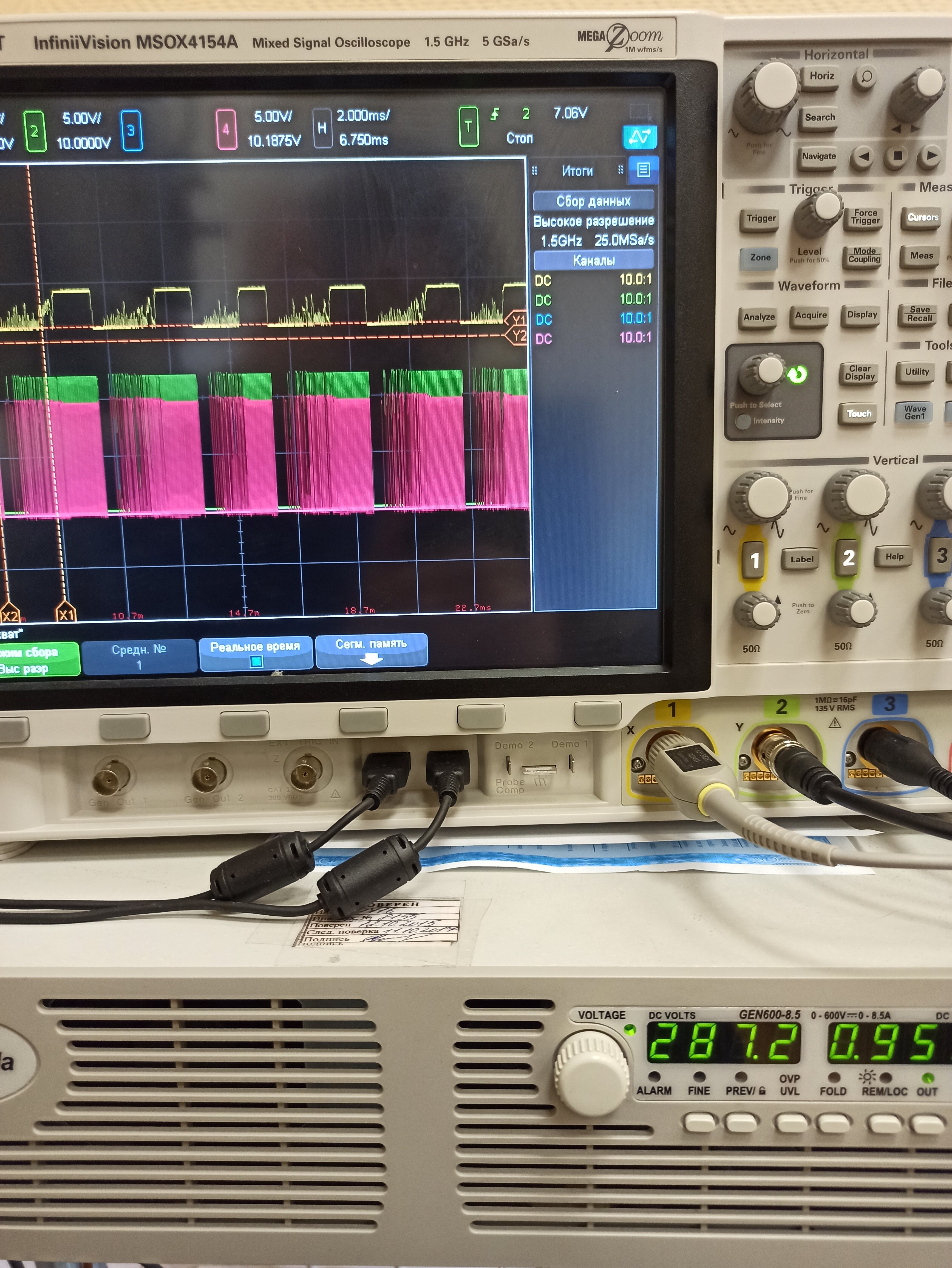
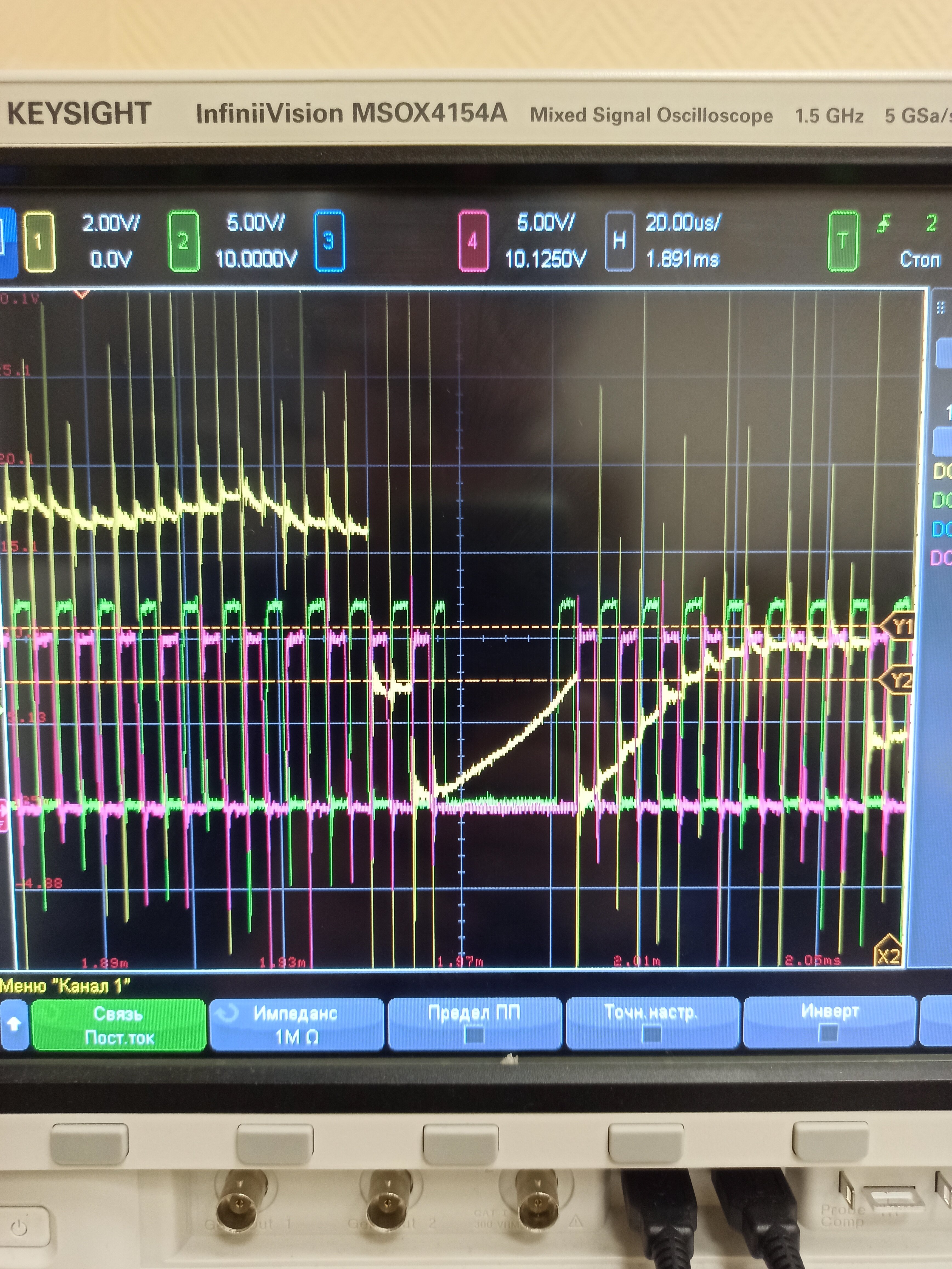
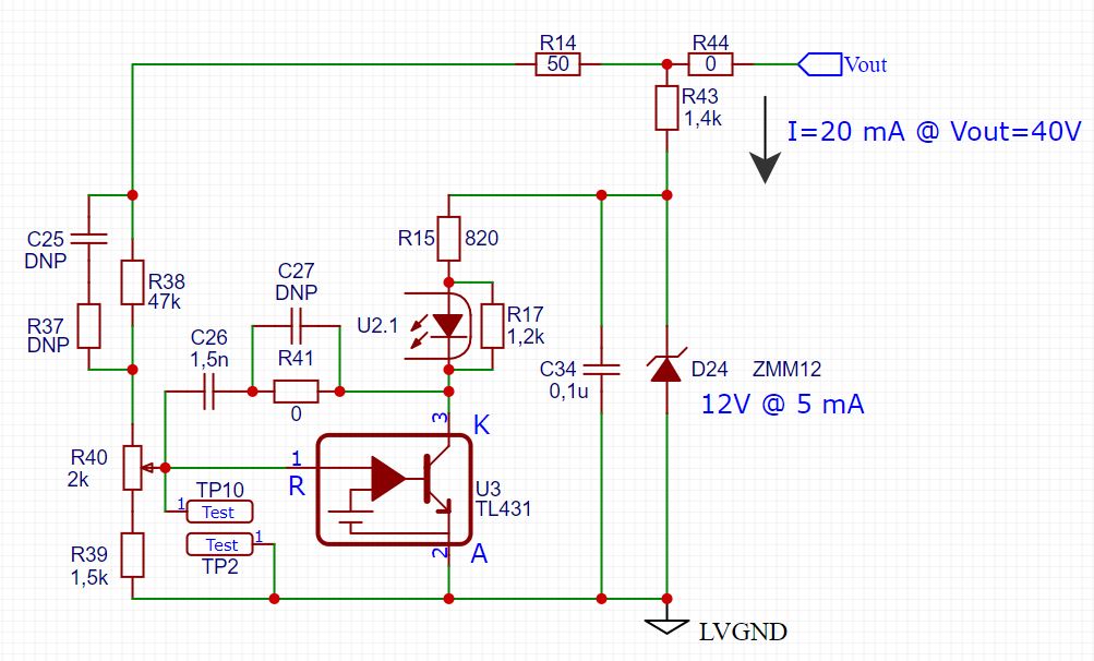
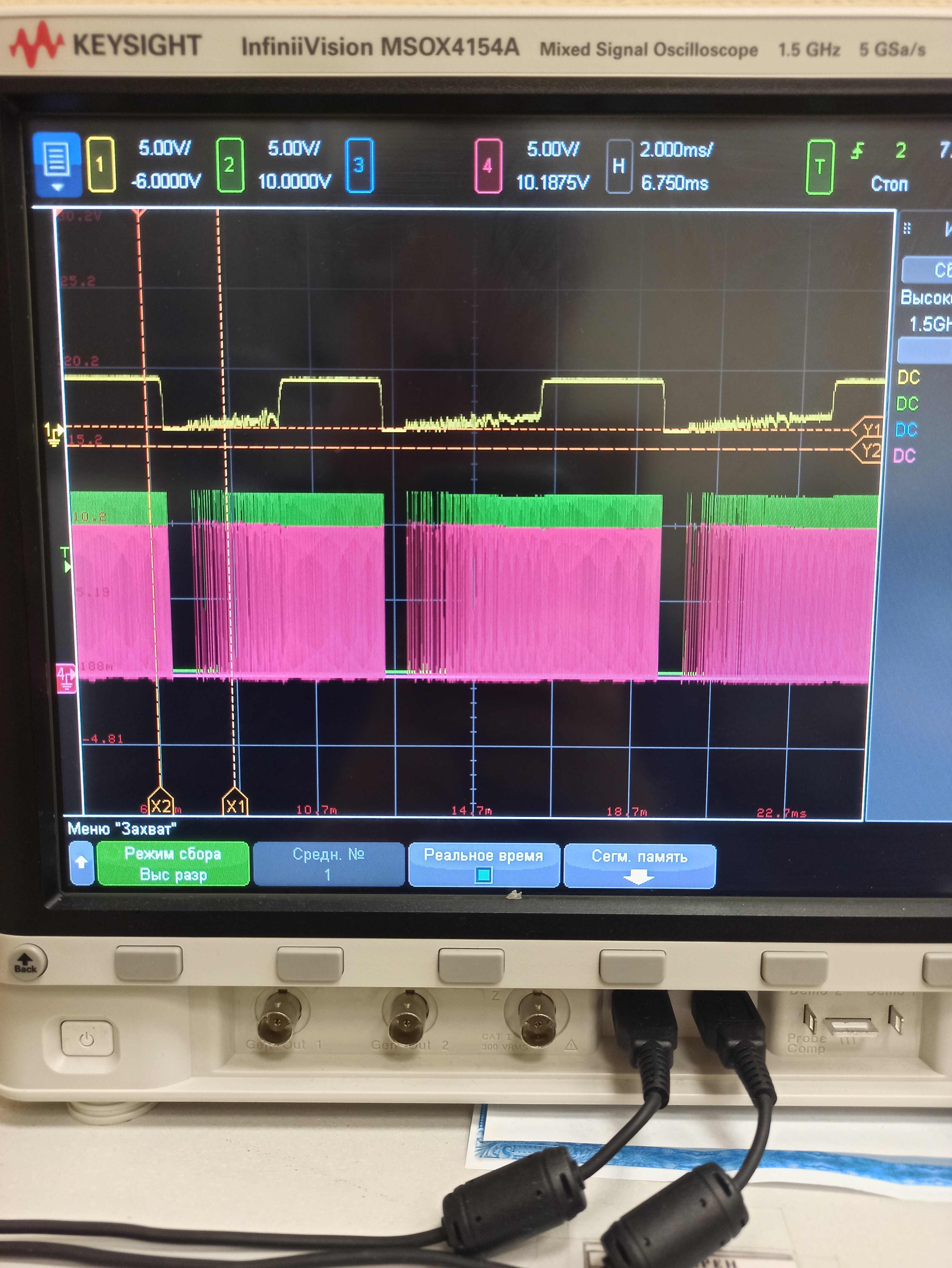
The problem occurs when converter starts to stabilize output voltage. The output voltage is somehow stable, but stabilization occurs at audible frequency so I can hear crackle and unpleasant noise. Waveforms shows that stabilization occurs in a few beats then EAP voltage hits no-load comparator threshold and disables the output. Then EAP voltage rises, PWM enables and everything is repeated again. I tried to put C26 in wide capacitance range (100p up to 0.1u) and this is didn't help much. Did anybody faced a similar problem, what is proper way to make it stable?
Please look at the waveforms and schematic. Yellow – voltage on EAP pin, green and pink is Vgs voltage of QA and QD mosfets. Load is ~6R:
1627292804175.jpg

1627294704092.jpg

1627292804178.jpg


fb2.JPG

fb1.JPG
 
Last edited by a moderator:

apart from having too much gain in the 431 ckt, are you running at no load? - 'cos this it what typically happens at no load ...
 

Yeah for some reason the feedback response is way too fast. Can't even see any significant changes in phase shift which would cause the output to change.

Are you sure you have enough capacitance on the output of the converter, and it has a low enough ESR?
 

Yeah for some reason the feedback response is way too fast. Can't even see any significant changes in phase shift which would cause the output to change.

Are you sure you have enough capacitance on the output of the converter, and it has a low enough E
Hello, mtwieg! The output capacitance is quite high and ESR is low. There is 6 capacitors 1000uF each at the output right after 14,5 uH inductor. Can it be too much capacitance…?

I am at a loss to say: is this is the way how not properly compensated TL431 / optocoupler feedback system works? Or it is another, more global problem? What do you think?

May it be not enough slope compensation for the sawtooth, or this should look different way if it is? (I put slope compensation at high value R27 and R26 and also, I added ~2V DC bias for my sawtooth via RP5).

I have built a type 2 compensation network with fast lane suppressed and plaid around with some values but only thing I have reached is that sound became quitter. Now if I increase load, at some point (above 600W) converter starting to work fine, and sound completely disappears.

I am using a PC817 without rating so it could theoretically have too much CTR? Or it should not influence so high…? idk. Planning to put PC817B instead.

I am wonder if there is relatively simple way to make converter work stable with type 2 compensation feedback, even at the cost of lac high frequency response? For example, a default values for feedback R and C, that guarantee converter will work stable.

fb2.JPG

fb.JPG
 

R41 = 220 ohm ( because the input divider R's are so low ) & C26 = 100nF

this gives a major pole where it is supposed to be - and will allow the converter to run ( also transpose the R & C for less RF pickup )

for improved response C25 = 22nF, R37 = 22k ( put these on later )
--- Updated ---

Also C34 = 1uF at least.
--- Updated ---

Also make the soft start cap on the chip for at least 0.5 sec, and fit a 1k res to the pin.
--- Updated ---

also C22 goes to 1nF else it will interfere with the loop.
--- Updated ---

Also a 10nF cap ( short leads or SMT ) from pin 9 to gnd, and pin 10 to gnd
 
Last edited:
R41 = 220 ohm ( because the input divider R's are so low ) & C26 = 100nF

this gives a major pole where it is supposed to be - and will allow the converter to run ( also transpose the R & C for less RF pickup )

can u explain pls, how do you calculate this values?
 

So, I have changed schematic according to your advices:
changed R41 = 220 Ohm
put C34=2.2 uF
put a 4.7 uF at SS pin (C21). (Didn’t placed 1k there because converter will not startup)
put C22 = 1 nF
and finally, I have added 10nF at pin 9 and 10 to GND.

The bad news is that nothing really changed. Converter still oscillates when it should stabilize its output voltage.
I connected a rheostat at the output and set it roughly to 6 Ohms. Then I turned on a converter at low input voltage (below 50 VDC) and started to rise it until the moment converter starts to stabilize the output. I took some waveform, so you can see what is going on.

Please sorry me for the croudness of these pictures, i havent measured it properly so signal appears too noisy but in fact it is bad probing and common mode noise...
Blue and pink is Vgs voltages on QA and QD transistors. Yellow is voltage at Ramp pin (3). Green is the voltage on the EAP pin (20).

Everything looks normal before stabilization:
Input 237VDC , out 41.63VDC (not stabilized yet)
1627560279097.jpg


When I came close to stabilization EAP voltage (green) slightly drops, but it is still should be higher than non-inverting input of EA (because of 0.8 offset at RAMP pin inside UCC3895).
Input 237VDC , out 42.36VDC (stabilization threshold)
1627560279093.jpg


As soon as I hit the stabilization threshold everything breaks and converter goes wild. I mean it is still maintaining the output somehow but it oscillates and makes audible noise.
Input 250VDC , out 42.17VDC (stabilization?)
almost nothing you can see at 2us/div
here what is hapining (2ms/div)
1627560279085.jpg

and zoomed in (still cycle skipping appears)
1627560279073.jpg
1627560279080.jpg
1627560279075.jpg


May we see the PCB layout, please?
Hello! Sure, here I also attached full schematic (last version) and top/bottom PCB views in .pdf.
 

Attachments

  • Schematic_PSFB_last.pdf
    195.5 KB · Views: 109
  • bot.pdf
    308.2 KB · Views: 95
  • top.pdf
    549.1 KB · Views: 107

2 things - is you slope comp working ? if not then this needs to be fixed other wise unstable above 45% phase shift

for smaller Lout you need lots of slope comp - it can be calc as at least half the down slope of the o/p current reflected to the CT output.

and - you need a lower gain opto, for starters lower R22 to 2k2
--- Updated ---

For example - with the circuit values shown you need to introduce at least 140mV per uS slope comp ( assuming 50:1 CT )

Does your circuit do this ? - also every time you fiddle with trimpot RP1 you would be changing the added slope comp

The peak o/p of the CT would appear to be about 2.35V - you really don't want to attenuate this ( as it worsens low load control )

you need to be adding about a volt max to this with the slope comp for stable operation above 45% phase shift, so 3.35Vpk after 5uS assuming 100kHz ...
--- Updated ---

Why is there a 2k pot into the ramp pin ?
 
Last edited:

Also do not put your scope probes directly on the pins or the tracks going to the points of interest - instead solder a 4k7 leaded resistor to the point of interest ( 4mm lead max to body of R ) then connect the probe to the other side of the 4k7, again shorten the lead to 10mm or so

this will stop you injecting RFI into the sensitive points with your probes.
--- Updated ---

which is part of the problem.
 

2 things - is you slope comp working ? if not then this needs to be fixed other wise unstable above 45% phase shift
I think my slope compensation should be fine since I used UCC3895 DS to build slope compensation circuitry and calculate all values. Here are my calculations:
calc.JPG

On PCB I used 1k resistors instead 3.3k to make slope compensation even larger, with sufficient margin, so it must not be problem with lac of slope compensation. Please see waveform when only UCC3895 is running (no HV applied at the input). We can clearly see biased compensation sawtooth:
Blue and pink is Vgs voltages on QA and QD transistors. Yellow is voltage at Ramp pin (3). Green is the voltage on the EAP pin (20).
1627657125550.jpg


Also I have changed PC817 by 817B and R22 to 2k2. RP1 is in its upper limit so we can assume it is not adding resistance to R73 and acts just like a 5k load at CST...
you need to be adding about a volt max to this with the slope comp for stable operation above 45% phase shift, so 3.35Vpk after 5uS assuming 100kHz ...
I tuned RP5 to make offset lower this time (please see first waveform). And I didn't really know what offset I will need so I just put the pot at this pin.

Also do not put your scope probes directly on the pins or the tracks going to the points of interest - instead solder a 4k7 leaded resistor to the point of interest ( 4mm lead max to body of R ) then connect the probe to the other side of the 4k7, again shorten the lead to 10mm or so

this will stop you injecting RFI into the sensitive points with your probes.
Yes, thank you for this advice, now I will measure only using 4k3.

But the problem is still exist. Converter does not stabilize properly. It all seems similar to what I have shown before:
1627657125542.jpg
1627657125538.jpg
1627657125535.jpg
1627657125517.jpg
 

Your basic problem (now & before) is that you have way too much gain in the f/b loop due to (mainly) the high gain of the opto

Also, ideally the slope comp should be designed such that the originating signal does not go negative

Can I have your rationale for feeding DC into the ramp pin ? it should really only have a slightly filtered I sig + slope comp

We always generate the slope comp from the GD pins as this always works nicely.

If you cannot find an opto with CTR = 20%,

then you need to further slow the control loop ( and lower the gain at mid frequencies ), and add damping, so C26 goes to 2 x 470nF in series, and place 4k7 across one of them

this will slow the f/b loop, reduce the gain at mid freq's and damp the response and should give stable ( if slow ) operation provided there is not some issue with RF getting into the control circuit. p.s. what does the diode o/p voltages look like ?
--- Updated ---

PC817B has CTR in the range 130% to 260% i.e. a lot of gain that you don't need.

the SFH615A-1 is a much better choice ( 40 - 80 % )
--- Updated ---

Also - if showing the gates drives, show the lower from each side so we can see the effective PWM applied to the Tx.
--- Updated ---

Also, the layout is a mess, to try and reduce some noise and stress on the fets, place 220nF, 400/630VDC film foil caps across each totem pole pair, so Drain ( HVDC+) on one to the source on the other ( HVDC - ) - on the back of the board with very short leads.

This will not unduly affect your current monitoring.

If L1 is an input choke to the HVDC caps - short it out for the present - as it will affect the stability of the whole converter.

where are the o/p diodes ?
 
Last edited:

Ok, thank you for your help. I will go to my local radio store and buy proper optocoupler to eliminate this gain problem. There is SFH615A-2 in stock, but I thik it is too much gain too so I will try to find SFH615A-1.
p.s. what does the diode o/p voltages look like ?
I am sorry, not sure that I got what o/p diodes is, can you give schematic designation or сlarify what you mean.

If L1 is an input choke to the HVDC caps - short it out for the present - as it will affect the stability of the whole converter.
I can understand that shorting shim inductor could affect the stability of the whole converter but what a point to make a working PSFB that cannot achieve ZVS? There is must be another way to make it stable, am I wrong?

Also, the layout is a mess
Can you please be more detailed on that? This is not a complete design but a bench model, so it has some disadvantages indeed. But I am trying my best to make it good so experienced and reasoned opinion will help me a lot in the future. If it won't take too much of your time cold you, please give us examples of mistakes made in my PCB and say why exactly you think that these are mistakes. It will help me improve my further designs and also be helpful for other people here.

To start with I can list mistakes I already knew about:
Bulk caps are too far from the fets (reason - parasitic inductance of this traces is a bad thing)
No gnd plane on the secondary side (reason - poor EMI)
Big current loops areas (reason - big loops is a good antenna which is a bad thing) btw not sure I can do much about this thing since the components are bulky and I already placed them as close as possible
--- Updated ---

Can I have your rationale for feeding DC into the ramp pin ? it should really only have a slightly filtered I sig + slope comp
UCC3895 DS p.39 "In peak current mode control the RAMP pin receives the current sense signal, plus the slope compensation ramp, through the 510-Ω resistor RRCS. The 10-kΩ resistor RRB provides approximately 250-mV offset bias. The value of this resistor may be adjusted up or down to alter the point at which the internal no load comparator trips."
I am not sure why they do this and how it exactly it "alters the point at which the internal no load comparator trips" but I think it has something to do with an 0.8V offset at ramp pin inside UCC3895, correct me if I am wrong please.
 
Last edited:

o/p = output
Now it is clear, thanks. Output rectifiers diodes is D21 and D22 it is ultrafast soft recovery diode 80EBU02, you can find them on pcb using this disignator. Due to the construction feature the cathode pin of it is connected to the PCB via thick wire. The waveform on these diodes looks common but has some oscillations (up to 180V), so I put RC snubber 1nF+220R as you told me. This reduced oscillations. I can took this waveforms if it will be useful.
 

Oh - I see L1 is the extra inductor for ZVS at lower loads, it is common practise to put resistors in series with the associated diodes to reduce ringing and current carrying time, say about 10 - 22 ohm in your case, 2W
 

R53 etc ( R turn on ) should be closer to 15 ohms
--- Updated ---

R43 needs to be at least 1W rated - 20mA x 28V = 560mW

it looks like it will die with the current foot print ...
 
Last edited:

Status
Not open for further replies.

Similar threads

Part and Inventory Search

Welcome to EDABoard.com

Sponsor

Back
Top