Porsche
Member level 1
Hello,
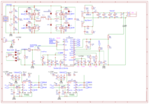
I am designing a CMC PSFB converter based on UCC3895. I ran into a problem with cycle-by-cycle current limiting.
When the voltage at the CS pin reaches the 2V threshold, the duty cycle starts to change rapidly and asymmetrically. This causes audible noise and could even lead to primary TX saturation (in this case 2.5V threshold kicks in, restarting the IC).
I expect that the duty cycle should change smoothly and symmetrically, reducing the output voltage when the load resistance decreases, thus limiting the output current. But that occurs only when the load resistance is too low, when duty cycle is already around 55% and less. From ~55% down to ~0% duty cycle changes smoothly and symmetrically. From ~80% down to ~55% duty cycle changes rapidly and asymmetrically.
Here's what I've tried so far:
Input voltage 350V, Output voltage 50V, Npri/Nsec=5, Ncs=100, current slope compensation ~0.19V/us, inductor down slope current transferred to the voltage is ~0.18V/us. Voltage control loop seems to work fine under all conditions. Stable 50V at the output without rapid duty cycle variations.
Yellow signal - voltage at the summing point (just compensating ramp), no input (350V) voltage applied.

Yellow signal - voltage at the summing point. Blue signal - output diode voltage. Red signal - output current. Converter runs, 50V and 6 Ohm load at the output.

Yellow signal - voltage at the R18 (40 Ohm). Blue signal - output diode voltage. Converter runs, 50V and 6 Ohm load at the output.

Yellow signal - voltage at the summing point. Blue signal - output diode voltage. Red signal - output current. Converter runs, 50 V at the output and current protection just about to trip.

Yellow signal - voltage at the summing point. Blue signal - output diode voltage. Red signal - output current. Converter runs, ~50 V at the output and current protection is tripping. Audible noise appears, you can see duty cycle variations on a blue waveform.


I am designing a CMC PSFB converter based on UCC3895. I ran into a problem with cycle-by-cycle current limiting.
When the voltage at the CS pin reaches the 2V threshold, the duty cycle starts to change rapidly and asymmetrically. This causes audible noise and could even lead to primary TX saturation (in this case 2.5V threshold kicks in, restarting the IC).
I expect that the duty cycle should change smoothly and symmetrically, reducing the output voltage when the load resistance decreases, thus limiting the output current. But that occurs only when the load resistance is too low, when duty cycle is already around 55% and less. From ~55% down to ~0% duty cycle changes smoothly and symmetrically. From ~80% down to ~55% duty cycle changes rapidly and asymmetrically.
Here's what I've tried so far:
- to remove oscilloscope probe from the summing point;
- to add more/less slope compensation;
- to add more/less filtering to the current signal;
- to add DC offset (~1V) to the summing point;
- to add/remove DC-blocking capacitor in series with main TX.
Input voltage 350V, Output voltage 50V, Npri/Nsec=5, Ncs=100, current slope compensation ~0.19V/us, inductor down slope current transferred to the voltage is ~0.18V/us. Voltage control loop seems to work fine under all conditions. Stable 50V at the output without rapid duty cycle variations.
Yellow signal - voltage at the summing point (just compensating ramp), no input (350V) voltage applied.
Yellow signal - voltage at the summing point. Blue signal - output diode voltage. Red signal - output current. Converter runs, 50V and 6 Ohm load at the output.
Yellow signal - voltage at the R18 (40 Ohm). Blue signal - output diode voltage. Converter runs, 50V and 6 Ohm load at the output.
Yellow signal - voltage at the summing point. Blue signal - output diode voltage. Red signal - output current. Converter runs, 50 V at the output and current protection just about to trip.
Yellow signal - voltage at the summing point. Blue signal - output diode voltage. Red signal - output current. Converter runs, ~50 V at the output and current protection is tripping. Audible noise appears, you can see duty cycle variations on a blue waveform.