Continue to Site

Welcome to EDAboard.com

Welcome to our site! EDAboard.com is an international Electronics Discussion Forum focused on EDA software, circuits, schematics, books, theory, papers, asic, pld, 8051, DSP, Network, RF, Analog Design, PCB, Service Manuals... and a whole lot more! To participate you need to register. Registration is free. Click here to register now.

PSD JTAG Programmer (F-link)

Status
Not open for further replies.

flexx

Member level 5
Joined
Feb 19, 2005
Messages
87
Helped
3
Reputation
6
Reaction score
1
Trophy points
1,288
Activity points
1,995
hi all , ihave (psd813f4a) FLASH IN-SYSTEM PROGRAMMABLE MCU

i need to update the software , and when i call the vendor theytold me i have to use F-link cable to upgrade the software on the system and theres a JTAG port from 14 pin on the system

i tried using the regular JTAG containing 74HC244 but it dosnt looks to connect to my system


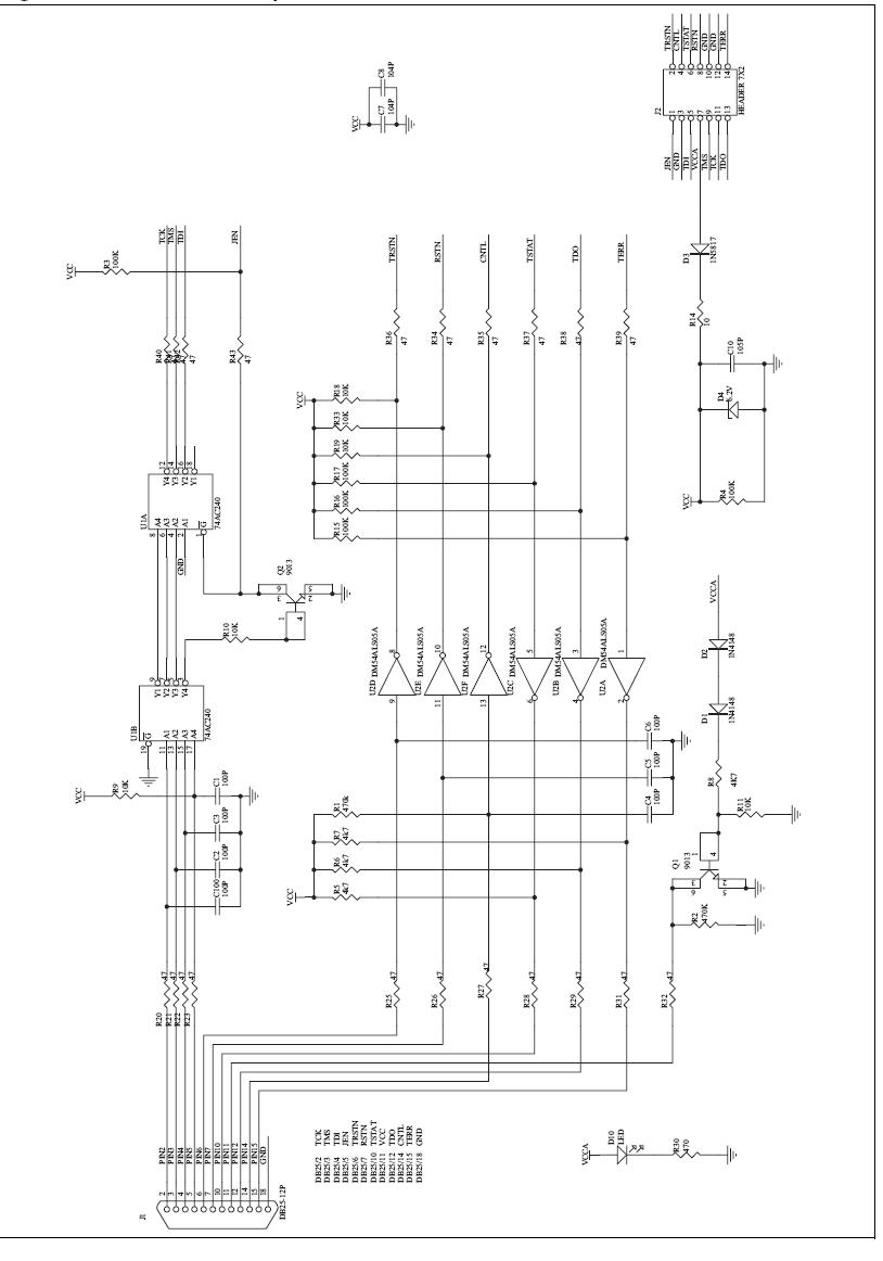
so i need to get the ( F-link ) cable to programe it and i got the schematics but i dont understand it
F-LINKcable.JPG


F-LINKcable
Programator/debugger mikrokontrolerów ARM STR91x, Flash PSD, uPSD oraz DSM

this is the schematics for this programmer
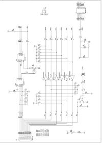


please help me
 
Last edited by a moderator:

This interface is not standard JTAG. It seems they have added several proprietary signals like "JEN" and "TSTAT" as well as several others.
The TMS, TCK and TDI signals are output from latches. This is why your standard 74244 pod did not work.
I would suggest building the circuit as shown. Without detailed knowledge of what parts of the circuit the JTAG software is using, you have to include it all. It is only a small handful of TTL, so it should not be too bad.
The next hurdle will be the software. Please be aware that software which interfaces via the parallel port can be rather fussy. Do not try using a USB to parallel converter. They will not work. You must have a parallel port on the motherboard or an expansion card. Next, the port settings are important. Often these JTAG software routines are targeted at only one port address. Make sure your PC matches that. Next, port type is important. Motherboards will often default to a bi-directional port, however this setting does to work with the software in some cases. Often the Standard or Output Only port version is required. These port settings are often in the BIOS, so be prepared to experiment and reboot the machine alot. Basically, you have to keep changing the parallel port settings until you find the combo that works. Be persistent, it will be dead as a doornail until everything is right.
 

thank you very much for you post but actually i dont have a background about how built it using ttl ? so any one can help me in this schematic it will be fine and iam sue this JTAG can be usfeul for any application

looking for answe
 

You don't really need to understand the schematic to build it. The two types of ICs that are used are the 74AC240 and the 74ALS05. (The schematic lists a 54ALS05A, but that is packaged in a harder to use format.) You can search the Internet for those two part numbers and find the datasheets and vendors that carry them. The "AC" and "ALS" are specific types in the TTL family. There are other types that can be substituted if those chips are not avaiable. However, it is best to follow the original design if possible.

Basically, you get some perf board, some DIP sockets, the resistors, capacitors and ICs and solder it all together using short pieces of wire. If electronic assembly is new to you, then perhaps a local tech school or junior college could help. Call the instructors, if you pay for the parts, they may make building this for you an extra credit project for one or more of their students. If the tech school idea does not work out, inquire at your local TV or electronics repair store. They probably know who to local electronic hobbyists are and can direct you to a local person that can help you build it.
 

thank you for your replying , ill try to built it and afte i analyze this schematics i found VCCA fom the JTAG Port and VCC ( This pat i cant understand actually how can i conect it )

ill try
 

VCCA is a voltage source provided from the psd813f4a board. (Pin7 of header J2). This voltage is reduced by a diode and resistor before becoming VCC. VCC is the power source for the rest of the circuitry. All power for the JTAG adapter comes from VCCA. The parallel port does not supply any power.

The TTL ICs also connect to VCC. However, this connection is implied and not explictly shown in the schematic. Take a look at the datasheets for the ICs and make sure you connect the VCC and GND pins.
 

ok i understand now the VCCA but why he Used Q1 (9013) and the same Q(9013) i know this is a transisto but why he connected like that 1 with 4 and 5 with 2 and 3 with 6 what is the point ?

ilooked to the schematic fo theis transistor it contains only 3 legs not 6 any explanaitions ?

egards
 

I think the pinout of these transistors have to do with the package they are in. I think the package has two transistors within it and the schematic symbol was built to show the either or connection.

Personally, I would substitute any small signal NPN transistor that I had available. The 2N2222 or the 2N3904 will work as well as many others. These transistors appear to only be signaling the presence or absense of signals. Q1 signals to the parallel port that the JTAG programmer is connected and powered up. Q2 signals to the psd813f4a board that the JTAG programmer is connected and that the JTAG software is running.
 

thats mean i can use only one tansistor and dont care about pin 1+4 and 2+5 and 3+6 it means i connect the tansitor only by pic 1 + 2 + 3 ??? and foget the 4+5+6

and do the smae with Q2 ??


looking for an answer thanking u
 

Yes, your understanding is correct, if you use the exact transistor and package that is in the schematic.
However, to use more connon transistors, all you have to do is match up the pin names and disregard any numbers. For BJT transistors, the three pins are named base, emitter, and collector (B,E,C). Take a look at
https://www.fairchildsemi.com/ds/PN/PN2222A.pdf
and you will see these pins labeled next to different packages of the part.
WIKI shows the pin names with symbol to complete the info. https://en.wikipedia.org/wiki/2N2222
Match the symbol and names to the symbol in your schematic and you are ready to go.
 

Status
Not open for further replies.

Part and Inventory Search

Welcome to EDABoard.com

Sponsor

Back
Top