Continue to Site

Welcome to EDAboard.com

Welcome to our site! EDAboard.com is an international Electronics Discussion Forum focused on EDA software, circuits, schematics, books, theory, papers, asic, pld, 8051, DSP, Network, RF, Analog Design, PCB, Service Manuals... and a whole lot more! To participate you need to register. Registration is free. Click here to register now.

Programming Atmega128 with ISP problem

Status
Not open for further replies.

Jman 31

Member level 2
Joined
Sep 18, 2009
Messages
49
Helped
0
Reputation
0
Reaction score
0
Trophy points
1,286
Activity points
1,675
I posted this with another thread that I had started, but I was afraid it may have gotten buried in that thread. I hope this is not against forum policy to post it here.

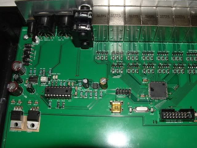
I have a question concerning this THIS SCHEMATIC that I designed. I built a prototype with out some of the peripherals just for test purposes. The guy that is programming it is having issues getting the **broken link removed** to talk to the chip. Could someone possibly look over the ISP and Atmega128 portion of my schematic to see if maybe I made a mistake in my design? Any advice would be greatly appreciated. (I used the footprint from an atmega103 to draw the schematic, but the pinout is the same). I wonder if it has to do with the RESET or PEN pins not being pulled high?

Here is a photo of the board:

DSCF00023.jpg
 
Last edited:

I guess, you would want to show a schematic supplementing your nice photo, to get an answer to your question.
 

I guess, you would want to show a schematic supplementing your nice photo, to get an answer to your question.

If you will notice the highlighted "schematic" in green in my first post, you will see that I did include it. :wink: HERE it is again though. You will also see that I included a link to the programmer we are using. :cool:

Edit: I went back and edited my post to make it a little more obvious. Sorry about the confusion.
 
Last edited:

I didn't notice the link. The ISP schematic seems fine, except for the missing nRESET pull-up resistor. You should also care, that the MOSI line isn't pulled down through the MIDI interface. Finally, there's a certain risk, that the ATmega CKSEL fuses have been unintentionally set to a wrong mode.
 

Thanks for the advice. I think I may have found the problem. When looking over my PCB, I notice that pin 53 (gnd) was not connected to the ground plane. I will fix that first and then if that doesn't do it, I will try the other stuff. I am thinking that that should do it though.

Thanks again,
J
 

The PEN pin description in the datasheet says:
PEN is a programming enable pin for the SPI Serial Programming mode, and is internally pulled high.
By holding this pin low during a Power-on Reset, the device will enter the SPI Serial Programming mode. PEN has no function during normal operation.

With a floating PEN pin you will not be able to program the device, you must apply a low.
I think the missing pull up resistor for reset pin will not be a problem for programming because the programmer will provide the high/low but you should use the pull up for normal operation to prevent any random resets.

Alex
 

It's true, that the quoted pin description for PEN can be found in the ATmega datasheet. But it's not listed in the ISP programming pin mapping and not connected by any ATmega circuit I know, neither my own nor others.

The confusion is cleared in the programming chapter:
As an alternative to using the RESET signal, PEN can be held low during Power-on Reset while SCK is set to “0”. In this case, only the PEN value at Power-on Reset is important. If the programmer cannot guarantee that SCK is held low during power-up, the PEN method cannot be used. The device must be powered down in order to commence normal operation when using this method.
Apparently all common programmers are working fine without using PEN, it's also not connected in the standard Atmel ISP connector. The internal pull-up resistor is specified in the datasheet, it should be sufficient for an unconnected pin. For nRESET, I suggested an external pull-up (because everyone uses it). I think, it's advisable, if longer traces are connected to the pin, but in the present design, it's not strictly required.
 

We are still searching for the answer. Fixing the ground on pin 53 didn't do it. I was hoping that PEN was the answer, but after what you said FvM I am afraid we are back to square 1. Not sure where to go from here. I guess we can try a pull-up on reset and see if that does it.
 

Did you program the specific chip before or is this the first time?
Have you tried the programmer before or with another chip to verify its operation?
What is the value or resistor R21 connected from the sck to the base of the transistor, is it 100 ohm like R19?
Have you checked the soldering of 128 for any shortcircuits (i see some fat solder joints but i don't know if it is just the photo) or have you used any liquid soldiering paste that needs to be cleaned?

Alex

---------- Post added at 15:35 ---------- Previous post was at 15:24 ----------

Why are you using such a low resistor to drive the base of the transistor (even if it is only for T2), you will have a current of about 40ma for each transistor and if the other resistors are the same you will have a problem.
What are the current requirements for the md outputs?
I think a resistor of 1K should be more than enough to drive the base of the transistors.

Alex

1. This is the first time we are trying to program this brand new chip.
2. Yes, I programmed one other chip with it and it seemed to function properly
3. yes all of those resistors are 100 ohm
4. Yes, I checked all of them with a continuity tester and they checked out OK. (I have shipped the board to my programmer, but I will have him recheck it again)

5. I used the 100 ohm just so as not to have a short when the transistor had power to it. What do you suggest, and why will I have a problem with it if you don't mind my asking? The **broken link removed** shows a base current of 1/2 amp for these transistors.
6. Current for MD outputs is about 500ma for each set of 3. So basically 200ma (maximum) per transistor or thereabouts.

Will the resistor value (R21) on T2 be a problem for that particular pin? Right now there is nothing on the MD outputs (they terminate to a jack), so the transistors are at an idle stage.

Thanks for taking the time to look this over. I have learned everything I know from Google so please bear with me if my knowledge is not up to par!
 
Last edited:

When you give a voltage to the base of the transistor, there will be a base-emitter current even if you don't have anything connected to the collector, think of the base emitter as a diode, you are giving 5v to the anode of the diode through a 100 ohm resistor and the cathode is connected to the gnd.
I think this resistor is definitely the problem because i doubt that the programmer can supply that current so it can't send the clock pulses, when the programmer is trying to send the clock pulses to the 128 it also drives (opens/closes) the transistor.
I said you have a problem because the 128 can't give that much current, if you open the 128 datasheet at page 318 (absolute maximum ratings) it says DC per I/O 40ma and VCC current 200-400ma.
All the current of the pins summed should not go above that VCC limit and you are already working near if not over the absoluter max current for the I/O pin.

Alex
 
Last edited:

Ahh, OK. That makes perfect sense now that you put it that way. So I should just be able to remove R21 for right now to at least see if the programmer will work, but i will need to change all of the resistors before I use it, correct?
 

I can't find the datasheet of your transistor to see the beta factor but if you use 1K base resistor the you will have a base current of about 4ma,
it will be more than enough to give a current of 200ma to the collector.

Alex
 
OK thanks for the very useful info!!!!
 

I think you have 38 pins connected to transistors, how many of them will be ON at the same time?

Alex

---------- Post added at 17:29 ---------- Previous post was at 16:45 ----------

I just saw your datasheet link, your transistor has a very high beta (above 500 up to 1A), if you look at page 7 figure 6 you will see that with 5ma base current you can have 1A in the collector with 0.25 voltage drop across the emitter/collector and 0.25W consumption that is in the safe area.
Since you are going to use currents up 500ma you can increase the resistor to the base to 2.2K (base current about 2ma)

Alex
 

OK, thanks you have been extremely helpful and I really appreciate it!
I will probably have a maximum of 15 pins on at any one time.
 

Alexan_e has actually recovered a serious design fault. It's manadatory to keep the VCC pins maximum rating.

It does however not explain the programming failure, because all outputs are tri-stated by default, and even if the chip has been programmed before with a code enabling the outputs (which could be easily detected with a multimeter, by the way), it would be immediately stopped by activating ISP mode.

So there must be another problem. If you managed to program the chip once, there's a certain risk that it has been damaged by the huge VCC current, but it sounds unlikely to me.
 

My main concern was the resistor R21 connected from the SCK pin to the base of the transistor T2,
so i asked if the value was 100 ohm as i thought (judging from the value of R19) and Jman 31 said that all the transistor base resistors were 100 ohm.
When the programmer send the clock to the SCK pin it also drives that 100 ohm resistor and i think the programmer can't give that current so the clock pulses are not correct.
I said that this was probably the cause of the problem, the VCC rating was the second problem i noticed that had to do with normal operation.
Jman 31 has also said that this chip on the circuit has never been programmed.

Alex
 

Alex, you hit the nail on the head. We are in the chip and programming! Thanks so much. I will address the design flaws, but at least we have some success.
 

Ok, so I have had time to stew on this for a bit and try to understand what we are talking about with the current consumption and the VCC. Basically, using the 2.2K resistors will drop it to a usable rating for what I am trying to do? So 2ma (current consumption to base using 2.2k resistor) X 15 (maximum pins at one time) = 30ma total? That is well below the rating of the VCC current (200-400ma). Am I thinking that out right? I also want to keep the LED strands as bright as possible so would a 1K or 1.5K be better as long as I stay below that vcc current rating?

Also, will the bigger resistor on R21 take care of the programming problem as far as the clock in concerned or does any pull on that pin change it? I could add a jumper that could be removed when programming and then added back when the pin needs to be used as I/O right?
 

Status
Not open for further replies.

Similar threads

Part and Inventory Search

Welcome to EDABoard.com

Sponsor

Back
Top