Continue to Site

Welcome to EDAboard.com

Welcome to our site! EDAboard.com is an international Electronics Discussion Forum focused on EDA software, circuits, schematics, books, theory, papers, asic, pld, 8051, DSP, Network, RF, Analog Design, PCB, Service Manuals... and a whole lot more! To participate you need to register. Registration is free. Click here to register now.

Process Corner variation in analog circuit.

Status
Not open for further replies.

imrankhanPNU

Member level 1
Joined
Feb 21, 2018
Messages
34
Helped
0
Reputation
0
Reaction score
0
Trophy points
6
Activity points
461
Hello,
I have designed an LPF demodulator. In a normal situation it's working fine, however when i carried out the Process corner simulation, the threshold voltage of MOSFET changes which is obvious, due to which MOSFET's operation region changes, ultimately change the output.

My question is :
1-How to deal /compensate for the process corner variation?

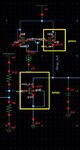
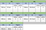
Note: I have attached the simulation circuit along with the table which illustrates variations in : Threshold voltage, Id, and region during different process corners.
Region: 0 "cutoff"; 1 "linear"; 2 "saturation"; 3 "subth"
Process Corners:
tm = Normal situation
wp = worst-case power
ws = worst-case speed
wo = worst case one
wz = worst-case zero
Thanks.
 

Attachments

  • 1.JPG
    1.JPG
    49.7 KB · Views: 127
  • 2.JPG
    2.JPG
    45.8 KB · Views: 167

"Corners" for digital timing / power "closure"
have not much to offer analog circuits. The
pre-baked cases aren't going to tell you
whether a gain drop is due to gm being low,
or Rout being low on one or the other species
of FET.

How you'd compensate (or re-center) has to
depend on the attribute and the mechanism
/ deviation that affects it. So you need to either
understand the process parameter(s) that
are responsible, so as to attack the appropriate
device (geometry, type, local topology) or
go and "shotgun" the design and cut-and-try
your way to a better recentering, a manual
"stimulus and response" effort of sorts. A more
sophisticated person might try sensitivity
analyses (if the PDK modeling tree supports
diddling process params and not just user
Spectre variables).
 
Thanks, @dick_freebird for your response.
Correct me if I am wrongly understood your point:
1-(Before baking/fabricating) It early to predict the variation of corner analysis in the case of analog circuits.
2- (Variation) Responsible process parameters need to be targeted, then try to play with it to recentered the process.

In my case threshold voltage of the MOS device is varying with process corners, I redesign the circuit for ws and wz corners but it was not working for wp and wo corners.
Then i tried to design the circuit for the wp and wo corner but it was not working for the ws and wz corners.
Because Vth in ws and wz =0.9V, Vth in wp and wo = 0.5V.

It's difficult to design the circuit for all four corners. ANy there any suggestion to deal with this issue?
 

It's difficult to design the circuit for all four corners. ANy there any suggestion to deal with this issue?
I think you would need to redesign the circuit design topology to be less sensitive to the corners.
That may mean a more complex circuit with feedback to minimize the sensitivities.
 
Status
Not open for further replies.

Similar threads

Part and Inventory Search

Welcome to EDABoard.com

Sponsor

Back
Top