ccarrot
Newbie level 6

- Joined
- Sep 19, 2007
- Messages
- 11
- Helped
- 0
- Reputation
- 0
- Reaction score
- 0
- Trophy points
- 1,281
- Activity points
- 1,399
Hi all:
I'm facing a problem about the Calibre LVS/PEX, I will describe it using this simple current mirror shown below, X and Y are same MOSFETs with width=16, nfing=2, m=1:

When I just do the layout with only one finger for both X and Y (w=16, nfing=1, m=1), and do the post-layout simulation, I injected 100uA to node Vb, it has no problem seen from the post-layout schematic: X will absorb 100uA and Y will source 100uA.
But when I use 2 fingers, the problem comes. The layout is:
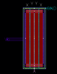
In this layout, the X and Y are in a single transistor which has w=32 and nfing=4, that means, X/Y are w=16, nfing=2 which is the same with the schematic above. ------ This is in my mind what is correct.
But when we do the LVS, it failed and showed property errors that X/Y has 2 fingers in the schematic but has 4 fingers in the layout:
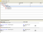
If change some MOS properties in the schematic, nfing is changed from 2 to 4 (layout doesn't change), then hen the LVS passes, which we think is not correct (but it passes!). I used this extracted CalibreView file to do the post-layout simulation, the current reduced to a half as seen the comparison below:
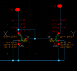
Pre-simulation, both X and Y have 100uA current:
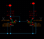
Post-simulation, the current reduced to only 50uA:
Does anybody know what would be the problem is and give some help? Thank you SO MUCH for any suggestions cuz I've been on this problem for days. Thank you!
I'm facing a problem about the Calibre LVS/PEX, I will describe it using this simple current mirror shown below, X and Y are same MOSFETs with width=16, nfing=2, m=1:

When I just do the layout with only one finger for both X and Y (w=16, nfing=1, m=1), and do the post-layout simulation, I injected 100uA to node Vb, it has no problem seen from the post-layout schematic: X will absorb 100uA and Y will source 100uA.
But when I use 2 fingers, the problem comes. The layout is:

In this layout, the X and Y are in a single transistor which has w=32 and nfing=4, that means, X/Y are w=16, nfing=2 which is the same with the schematic above. ------ This is in my mind what is correct.
But when we do the LVS, it failed and showed property errors that X/Y has 2 fingers in the schematic but has 4 fingers in the layout:

If change some MOS properties in the schematic, nfing is changed from 2 to 4 (layout doesn't change), then hen the LVS passes, which we think is not correct (but it passes!). I used this extracted CalibreView file to do the post-layout simulation, the current reduced to a half as seen the comparison below:
Pre-simulation, both X and Y have 100uA current:

Post-simulation, the current reduced to only 50uA:

Does anybody know what would be the problem is and give some help? Thank you SO MUCH for any suggestions cuz I've been on this problem for days. Thank you!