Continue to Site

Welcome to EDAboard.com

Welcome to our site! EDAboard.com is an international Electronics Discussion Forum focused on EDA software, circuits, schematics, books, theory, papers, asic, pld, 8051, DSP, Network, RF, Analog Design, PCB, Service Manuals... and a whole lot more! To participate you need to register. Registration is free. Click here to register now.

Problem with the gain plot of a charge amplifier

Status
Not open for further replies.

taik

Member level 3
Joined
Oct 22, 2007
Messages
58
Helped
1
Reputation
2
Reaction score
0
Trophy points
1,286
Activity points
1,604
Charge Amplifier

hi, hope someone can advise me on the problem i am facing.

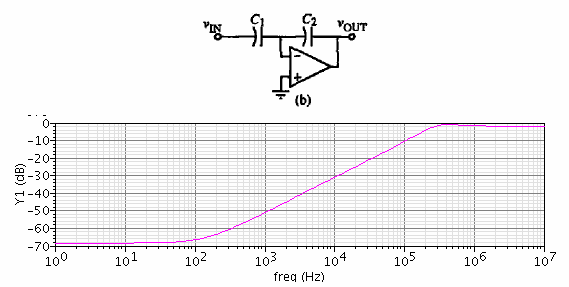
below shows a circuit which the gain is c1/c2. however, i am unable to get this gain. the gain plot is shown. it should be an all-pass tf with gain C1/C2 but i am not getting anything close.

can anyone tell me what's the problem?

c1=50p, c2=1p, open-loop gain of op-amp=60dB


ca.gif
 

Charge Amplifier

how are you biasing the input node
 

Charge Amplifier

one dc source at pos and neg node each...
 

Re: Charge Amplifier

I think you just don't have a DC operating point. Check the voltage on the negative input.
Maybe you can put a big resistor parallel to C2.
 

Charge Amplifier

try posting ur schematc/test_bench
 

Charge Amplifier

Looks like an operating point problem.
And what is DC source at pos and neg each? This is usually AC short to ground.
I think at least a detailed diagram is needed to show how you bias the amplifier.
 

Re: Charge Amplifier

taik said:
........ it should be an all-pass tf with gain C1/C2 but i am not getting anything close

Besides the bias problems already mentioned such a circuit never will work as an allpass filter. An allpass is a device with constant gain and frequency dependent phase.
 

Status
Not open for further replies.

Part and Inventory Search

Welcome to EDABoard.com

Sponsor

Back
Top