Continue to Site

Welcome to EDAboard.com

Welcome to our site! EDAboard.com is an international Electronics Discussion Forum focused on EDA software, circuits, schematics, books, theory, papers, asic, pld, 8051, DSP, Network, RF, Analog Design, PCB, Service Manuals... and a whole lot more! To participate you need to register. Registration is free. Click here to register now.

Problem with synchronous buck converter

Status
Not open for further replies.

dtruong

Newbie level 4
Joined
Jun 5, 2022
Messages
6
Helped
0
Reputation
0
Reaction score
0
Trophy points
1
Activity points
58
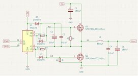
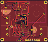
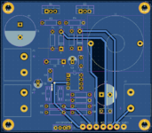
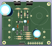
Hi, I’m doing a synchronous buck converter using half bridge driver IR2109 () to step down 200 VDC output from my PFC circuit to around 80VDC. I made a PCB and tested out with Vin = 12 VDC, pulled the to high and drove the IN pin by a 100 kHz PWM signal with 50% duty cycle from the Arduino Uno. The board worked fine, and I got a 6 VDC output. Then I tested it with 200 VDC from the PFC, and the traces from the input bulk capacitor to the high side MOSFET, and between the two MOSFET blew up. Both MOSFET were broken as well. So, what was wrong here?

Could it be the fix deadtime in the IR2109 wasn’t enough to protect MOSFET from shoot-through when Vin = 200VDC, even though it worked with Vin = 12VDC?
 

Attachments

  • buck converter.jpg
    buck converter.jpg
    68.8 KB · Views: 442
  • Infineon-ir2109-DS-v01_00-EN.pdf
    352.3 KB · Views: 131

Hi
So, what was wrong here?
Obviously overcurrent.

But what cause the overcurrent?
* load current? You did not tell anything about the used load.
* saturated inductor
* overvoltage spikes killed the MOSFET (due to bad PCB layout / wrong circuit / wrong part selection

My recommendation:
Others had identical problems, thus there are a lot of thereads. All has been discussed before.
--> read through them
Also there are application note provided by the semiconductor manfacturers. They provide more detailed design considerations. --> read through them.

--> show us your PCB layout.
--> give details about the used inductor and capacitors

--> in future do tests with a suitable light bulb in series with the power line input (VIN node)

***
What I´d design differently: (means: this are no mistakes)
* add a bulk capacitor and a fast ceramics capacitor at 12V_VCC node close to the diode
* replace the D2, D3 diodes with "fast" diodes. You don´t need the high voltage rating here
* replace R3, R4 with 10k
* add a fast capacitor at VIN node close to the MOSFET
* consider to add fast diodes in parallel to the MOSFETs

Klaus
 
In addition to the points already mentioned: IR2109 fixed dead time is surely not too short, rather unsuitably long for a 100 kHz switcher.

A circuit of unknown performance should be first operated with a current limited power supply and increasing voltage, carefully watching waveforms and current consumption. If you lack of a suitable high voltage lab supply, there's a problem.

The output capacitor is able to cause inductor saturation and large overcurrents if you don't ramp the pwm on start.

Finally, a popular cause of switcher failure at higher supply voltage is crosstalk of switching noise to the control circuit. We should see the circuit layout.
 
  • Like
Reactions: dtruong

    d123

    Points: 2
    Helpful Answer Positive Rating
Hi,
Here are the layout of my PCB. I wanted the maximum output current at 2A and I tried to minimized the power line trace width at 1.5 mm, which now I think it is not enough.
Please ignore the optocouplers in the left side of the IR2109, which at first I used to isolate the control signal from the Arduino, but the component I chose not switching fast enough so I end up connect the PWM signal directly to the IR2109.
give details about the used inductor and capacitors
My output capacitor (180uF/200V): https://www.nichicon.co.jp/english/products/pdfs/e-upt.pdf
My inductor (820nH): https://www.bourns.com/docs/Product-Datasheets/2300_series.pdf
If you lack of a suitable high voltage lab supply, there's a problem
Yes, I don't have any high voltage supply so I kind of blind when testing with increase voltage
 

Attachments

  • PCB top layer.png
    PCB top layer.png
    43.1 KB · Views: 112
  • PCB bottom layer.png
    PCB bottom layer.png
    40.1 KB · Views: 96
  • PCB layout.png
    PCB layout.png
    138.5 KB · Views: 122

Hi,
Thats high voltage.....are you using SiC diodes and FETs?
Severe rev recovery if not.

Note that the Boost PFC is never done with sync rects....likely for same reason sync buck usually isnt...unless with sic.

Also, what is your power level?...then i simulate for you and give the sim....in LTspice...always always get a sim going b4 going to hardware.

Maybe your driver doesnt give enough dead times for your fets at high V...where the miller makes the Stray c look bigger
Hi,
I'm not using SiC components, just Si one. Is this a requirement to go with SiC for sync buck?
My PFC (500W) takes 120 VAC/60Hz and output 200VDC. Then I fed this to the sync buck to get down to 80VDC/2A max current
 

Depending on switching speed, and size of choke - it is pretty easy to blow up the bottom mosfet - (followed closely by the top one) due to reverse recovery effects in the bottom mosfet, say you have allowed ~ 100nS dead time - then for a short time the diode in the bottom mosfet is conducting prior to the top mosfet turning on - if this top fet turns on too fast - it can cause gate rise on the bottom fet gate, and also cause failure due to exceeding the dv/dt limits on the bottom fet - when its internal diode snaps off and the voltage rises rapidly

you need to read up about all these effects ...
--- Updated ---

try limiting your boost ckt to 180VDC - this will help with switching losses.
 

Some questions haven't been yet answered.
You are actually using slow 1N4004 for the bootstrap supply?
Did you use pwm soft start?
 

Just looked at the inductor - it is not rated, for 80V 2A out - the L should be 5A rated at least

ensure you have a current limit and soft start on the buck.
--- Updated ---

try limiting your boost ckt to 180VDC - this will help with switching losses.

you cannot use 1N4004 diode for boot strap ( or gate drive either really )
--- Updated ---

also you cannot take the switching node below -5V in the buck ckt ( due to poor layout and little close decoupling ) else you run the risk of blowing up the gate driver - Fig 29 on data sheet.
 
Last edited:

Some questions haven't been yet answered.
You are actually using slow 1N4004 for the bootstrap supply?
Did you use pwm soft start?
I didn't use soft start or current limiter before the buck.
For the diode, I will change it to the UF4004.


a current limit is where you sense the output current and use this sensed signal to reduce the PWM in order to limit the current to a max value - to protect the semi's

If your load can never short or draw more than the 2A stated - then you don't need it.
 

..if i was you i'd get it runing as non-synch buck first.
Also, does your controller avoid switching the low fet on when in light load.....if not it couldl short the output cap
 

i'd get it runing as non-synch buck first
I tried the non-sync buck, but the IR2109 not working properly with that config so I need another driver like the IR2117.
Also, does your controller avoid switching the low fet on when in light load.....if not it couldl short the output cap
I'm not sure about this.
 

..Yes in light load , when the inductor current goes to zero in the switch sycle, its a problem....synch bucks turn the bott fet on when the top fet is off.......but in light load...you dont want the bott fet on for all of the time that the top fet is off......because when the L current has zeroed.......if your bott fet stays on, then its a big problem.....as the L current will build up big time in reverse.
 

.if your bott fet stays on, then its a big problem.....as the L current will build up big time in reverse.
What you describe, build up a reverse inductor current under light load condition is just what we call synchronous buck operation. It slightly increases converter losses but also keeps pwm gain constant, a big advantage in dynamic behaviour. Keeping synchronous operation over the full load range is well possible and should also work for the present design after applying the suggested corrections.
 

...Ahh thanks yes......and it needs one of the controllers that supports this.........ie not go into burst mode in light load...just switches the fets at f(sw) all the time....but yes, i see youre going to do it with one of those very controllers........using the arduino with fixed duty cycle.......as we know, in light load or no load, some synch bucks are in danger of leaving top fet off for long time....and bott fet the opposite of that....ie, ON for a long time........thats when the disaster can happen.

Since OP is using Arduino....i am sure they know this.....when you disable the sync buck......leave both top and bottom fets off.........normal sync buck logic says "IF top FET ON, THEN bott FET off...and vice versa"......this can cause a problem when you go into disable.
 
Last edited:

Status
Not open for further replies.

Similar threads

Part and Inventory Search

Welcome to EDABoard.com

Sponsor

Back
Top