dompa
Newbie level 1
Hello.
I have designed and made my own three-phase inverter and I am currently testing it with a regulated DC supply, but recently one of the MOSFETs failed.
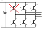
I replaced the MOSFET and checked the gate signals with a scope.
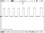
When I checked the signal on the bottom MOSFET gates, I see a constant PWM signal of 12V, independent of the DC supply, which is good.
ET gates, the peak voltage PWM keeps rising when I rise the DC supply!!
I got almost to 20V peak with 10V DC supply.
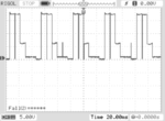
That's why the MOSFET died the first time.
So, my question is, what could be the reason the gate voltage keeps rising?
Thanks in advance.
I have designed and made my own three-phase inverter and I am currently testing it with a regulated DC supply, but recently one of the MOSFETs failed.

I replaced the MOSFET and checked the gate signals with a scope.
When I checked the signal on the bottom MOSFET gates, I see a constant PWM signal of 12V, independent of the DC supply, which is good.

ET gates, the peak voltage PWM keeps rising when I rise the DC supply!!
I got almost to 20V peak with 10V DC supply.

That's why the MOSFET died the first time.
So, my question is, what could be the reason the gate voltage keeps rising?
Thanks in advance.
Last edited by a moderator: