Continue to Site

Welcome to EDAboard.com

Welcome to our site! EDAboard.com is an international Electronics Discussion Forum focused on EDA software, circuits, schematics, books, theory, papers, asic, pld, 8051, DSP, Network, RF, Analog Design, PCB, Service Manuals... and a whole lot more! To participate you need to register. Registration is free. Click here to register now.

Problem with optocouplers in the design of a variable frequency drive.

Status
Not open for further replies.

kikeTC

Newbie level 4
Joined
Jan 26, 2023
Messages
7
Helped
0
Reputation
0
Reaction score
0
Trophy points
1
Activity points
63
Hello everyone, my name is Enrique and I recently discovered this fantastic forum.
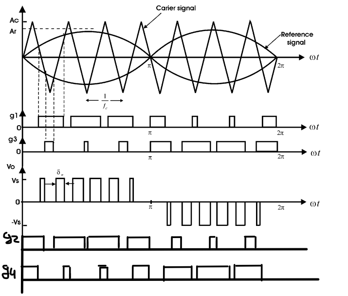
I wanted to write about a Variable Frequency Drive I'm working on. It is based on an Arduino (later I will migrate it to a stm32) using the unipolar spwm technique (4 kHz).
Captura de pantalla 2022-12-15 153328.png

Through the timer I compare two sinusoidals that are updated at each interruption of the timer. Subsequently, through a not gate (74ls04) I get the 4 necessary signals.
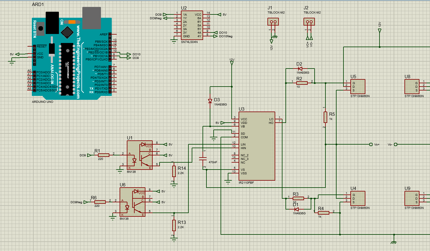
imagen_2023-01-26_161544680.png

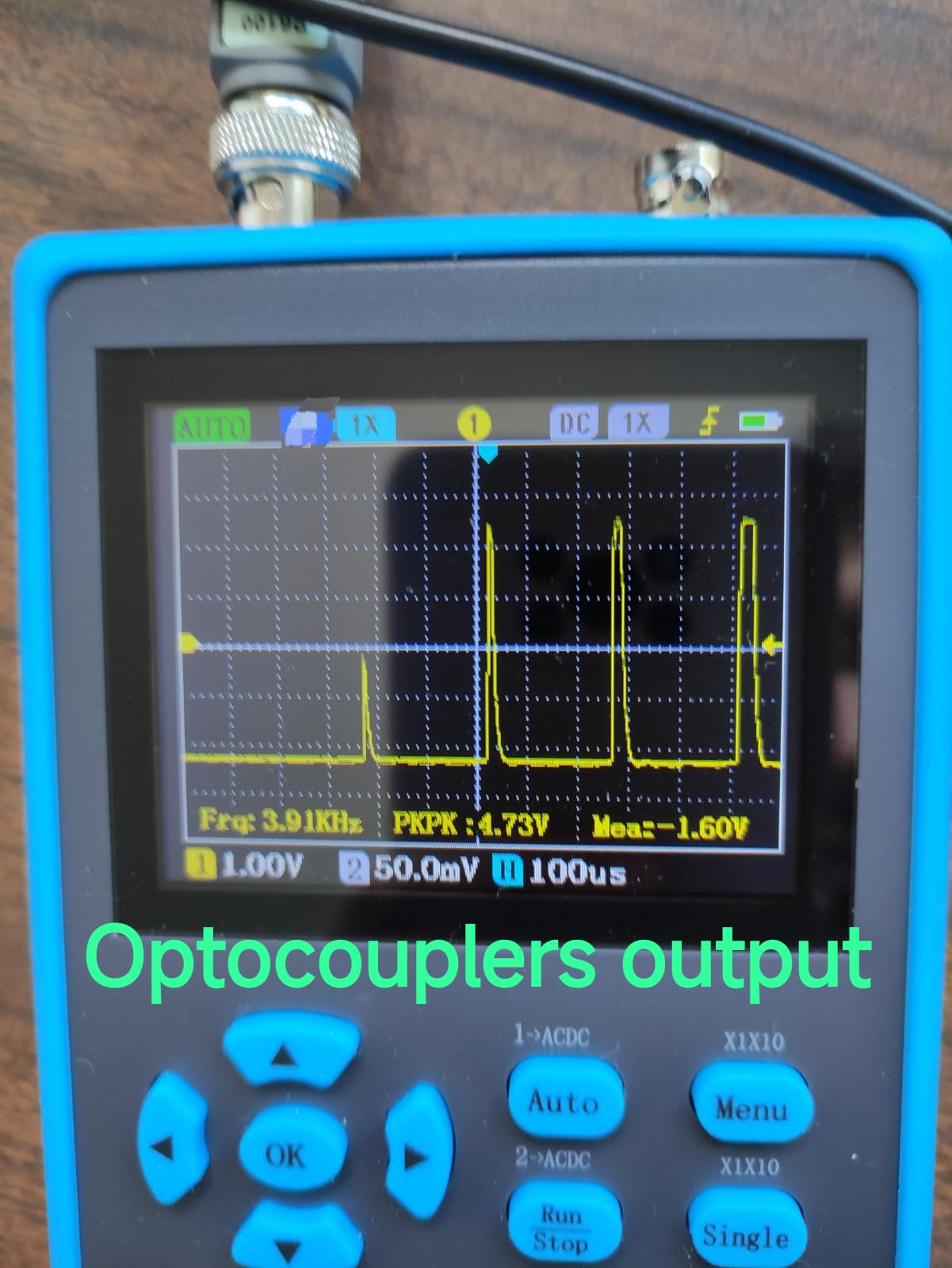
The problem comes when I pass the signals through some fast optocouplers (6N136)... These optocouplers do not imitate the shape of the pwm perfectly and it causes the mosfets to not switch correctly.
WhatsApp Image 2023-01-26 at 4.20.25 PM (1).jpeg

1. Are optocouplers essential to control ACIM?
2. If so, do I have something wrongly connected or some value of the resistors that causes this delay?
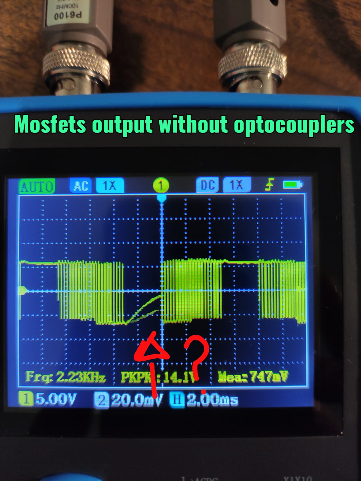
3. If I don't use them, the switching is correct except in the negative half cycle of the sinusoidal that does something strange, what could be due to it?
WhatsApp Image 2023-01-26 at 4.23.22 PM.jpeg
 

Optocouplers or other isolation means is required if you want to isolate driver from power circuit. With common ground as shown in your schematic, it serves no purpose.

6N136 can work for medium speed inverter, but in your schematic, LED drive current is a bit too low if we look at gauranteed current transfer ratio. Also asymmetrical delay causes potentially overlapping gate drive and shoot through. You'd better shift the inverter to the OC output, this would also save one OC per half bridge. Or generate separated Hi and Lo control signals with intentional dead time.
Thanks for your answer, I am new to electronics and these answers help me a lot.
Regarding the ground, you are right, I should use a 5V source external to the Arduino.
Regarding the CTR, the current through the diode is 16mA, which is what is used in the datasheet. Should I use a smaller resistor like 170 ohms?
imagen_2023-01-26_174233868.png

Lastly, I don't understand what you mean by: "Also asymmetrical delay causes potentially overlapping gate drive and shoot through"
Should I use the bipolar spwm technique, worse but easier to implement?
 

Those opto's you mention are not " fast" in the conventional sense - read the data sheet carefully

fast would be 200nS rise and fall times on the output ...
 

Those opto's you mention are not " fast" in the conventional sense - read the data sheet carefully

fast would be 200nS rise and fall times on the output ...
Hi, thanks for your response.
The best configuration I have achieved has been the following:
imagen_2023-01-28_140320782.png

However, the rise time is 3 microseconds and the fall time is 1 microsecond.
This is far from the maximum 0.8 microseconds reported in the datasheet.
What am I doing wrong?
 
Last edited:

Hi,

What am I doing wrong?
Rather simple: You did use a different circuit with different part values.
The datasheet shows the test conditions including circuit and part values.

To me it´s quite expectable: Different circuit --> different results.
Doesn´t this make sense?

Klaus
 

You did use a different circuit with different part values.
I'm sorry but I'm starting in electronics and this is my first serious project. I still have many things to learn.
Could you explain it a bit more? What part values do I have wrong?
 

Hi,

This question implements that you read the datasheet and use the exact same circuit and values?
Just to be clear: You want to validate "swtiching times" thus you have to refer to the datasheet schematics "switching times".

What datasheet exactly do you use? Give a link to it. (manufacturer site)

Klaus
This is the datasheet I'm using and it doesn't specify any load resistor value or at least I couldn't find it.
From figure 10, I think it uses a pulse generator with a duty of 10% and 5Vpk.
 

Hi,

Where do you have the "0.8us" value from (post#5)?
Isn´t in the same row a column called "Test conditions"? I see: "IF = 16 mA, VCC = 5 V, RL = 1.9 k Ω"

Klaus
 

Hi,

Where do you have the "0.8us" value from (post#5)?
Isn´t in the same row a column called "Test conditions"? I see: "IF = 16 mA, VCC = 5 V, RL = 1.9 k Ω"

Klaus
Yes, in the circuit there is a RL of 2.2K, close to 1.9K
In the datasheet it shows 0.8us maximum of tphl or tplh:
imagen_2023-01-28_160053661.png
 

Hi,

Maybe I´m a bit dumb.

* Why did you connect "B" with 10k? Where is this shown in the datsheet?
* did you set IF = 16mA? I can´t see this.
* did you drive with R_source = 50 Ohms? I can´t see this.
* did you measure it at a threshold of 1.5V?

If you don´t follow the datasheet you can´t compare the results. I can´t do this for you.
I don´t want to read the whole datasheet for you and write the contents in this thread.

I don´t see how you come to the rise and fall times you mention in post#5. In the simulation? In a true circuit?

Klaus
Hello, thanks for your reply.
It's normal that you don't, but you helped me a lot.
I used a 10k resistor on pin 7 because there is a floating point there. Many data sheets do not mention it but I saw a video where it was recommended and the improvement is brutal.
Here I leave the video:
The circuit is real and I measured it with an oscilloscope.
--- Updated ---

R2 = 1Meg, R3 = 680 ohm, put 150pF and 22 ohm ( in series ) across R1.
Thanks,
I will try with those values that you give me.
If it still doesn't work with those values, I'll change to the 6n137 optocoupler which is much much faster.
 

Hi,

In post#5 you complaind about the difference of speed values compared to the datasheet.
Thus I referred to the datasheet test method.

Now it seems you are interested on improving speed at all (independent of datasheet values and circuit)

Klaus
 

I used a 10k resistor on pin 7 because there is a floating point there. Many data sheets do not mention it but I saw a video where it was recommended and the improvement is brutal.
Opto coupler circuit design needs to take account of type variations, temperature dependence and aging. Deviating from manufacturer application circuit based on empirical measurements with a single exemplar (or a Youtube video claiming these results) is bad engineering.

Connecting a base-emitter resistor reduces current transfer ratio and thus invalidates the manufacturer specification of minimal drive current and load resistor.
 

Your schematic has single-ended 12V supply. It's suitable for a low voltage driver which biases mosfets directly.

Your gating scheme shall operate the H-bridge so that it acts as a buck converter in one direction during one-half of the cycle...
Then reverses operation so it acts as a buck converter in the other direction during the second half of the cycle.

This reply may be off the mark in case you want isolation because you expect severe high voltage spikes, etc. In any case this simplified simulation illustrates. Nmos & Pmos are installed in positions so that control waveforms are readily obvious.
Red wires are positive polarity (at the moment the screenshot was snapped). Waveforms sometimes go slightly into the negative region. The load gets bipolar AC.

I made plain comb-like pulses because it's easier than mimicking sine PWM. A series inductor acts in the typical smoothing filter role for the load.

pulsed gating 4 mos H-bri 12V load w inductive smooth.png
 

Status
Not open for further replies.

Part and Inventory Search

Welcome to EDABoard.com

Sponsor

Back
Top