FreshmanNewbie
Full Member level 6
I'm using this MOSFET driver IC.
Below is the schematic of the high side:

I followed figure 6-3 and 6-5 for the ICs schematics connections.
I have not populated the LED branches off of the gate outputs on all of the drivers (high side and low side). One thing I noticed in capturing this data was that the Vboost signal starts where it is supposed to be (~37V) but then drops down to near system voltage (~24V) and never recovers to what it should be after the first pulse. This seems to me to be the root of this issue however I am not sure how to address it. I would imagine that the voltage at the Vboost pin should recover back up to the ~37V it was before the input pulses started.
These screenshots were taken with a 2.7nF boost capacitor. I had tried the configuration previously mentioned with 10nF as the boost capacitor connected to Vdd. The first few cycles were elevated but they decayed quickly to the system voltage (i.e no boost). So it looks like it helped a little with the boosting but ultimately decayed in the same way the 2.7nF boost capacitor did.
I have noticed that while this circuit runs in its current state, the high side MOSFET is getting warm quickly during operation, likely due to a weak turn on voltage not turning the MOSFET on all the way.
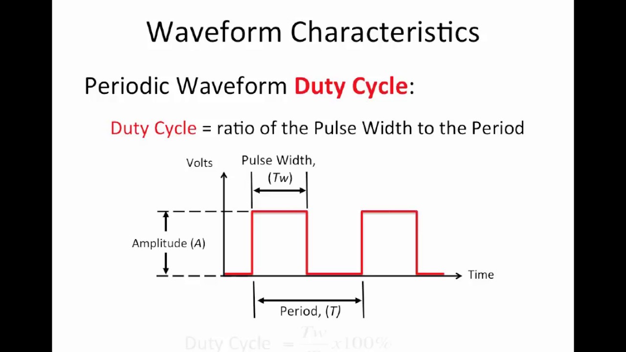
There is a drawing to show the voltage across the load. I am currently using a 1.8 ohm resistor to simulate the load that will be present in the final application, a 24VDC brushless DC motor. Since it is a 1.8 ohm resistor, the load current was determined by dividing the voltage pulse amplitude by the resistance. Since the signal is ~50% duty cycle the practical current would actually be half of that calculated result.


Below is the schematic of the high side:
I followed figure 6-3 and 6-5 for the ICs schematics connections.
I have not populated the LED branches off of the gate outputs on all of the drivers (high side and low side). One thing I noticed in capturing this data was that the Vboost signal starts where it is supposed to be (~37V) but then drops down to near system voltage (~24V) and never recovers to what it should be after the first pulse. This seems to me to be the root of this issue however I am not sure how to address it. I would imagine that the voltage at the Vboost pin should recover back up to the ~37V it was before the input pulses started.
These screenshots were taken with a 2.7nF boost capacitor. I had tried the configuration previously mentioned with 10nF as the boost capacitor connected to Vdd. The first few cycles were elevated but they decayed quickly to the system voltage (i.e no boost). So it looks like it helped a little with the boosting but ultimately decayed in the same way the 2.7nF boost capacitor did.
I have noticed that while this circuit runs in its current state, the high side MOSFET is getting warm quickly during operation, likely due to a weak turn on voltage not turning the MOSFET on all the way.
There is a drawing to show the voltage across the load. I am currently using a 1.8 ohm resistor to simulate the load that will be present in the final application, a 24VDC brushless DC motor. Since it is a 1.8 ohm resistor, the load current was determined by dividing the voltage pulse amplitude by the resistance. Since the signal is ~50% duty cycle the practical current would actually be half of that calculated result.