Continue to Site

Welcome to EDAboard.com

Welcome to our site! EDAboard.com is an international Electronics Discussion Forum focused on EDA software, circuits, schematics, books, theory, papers, asic, pld, 8051, DSP, Network, RF, Analog Design, PCB, Service Manuals... and a whole lot more! To participate you need to register. Registration is free. Click here to register now.

Problem with IC gate driver of a mosfet

Status
Not open for further replies.
No it's the correct pin! By supplying the driver, before even i turn off the low side so to be able the Cbst to charge, i have 10V and something more on HO.
 

I think you might find that H0 is just floating high when you measure it static. If you turn on the low side, it will go low.
When it is running, it will work as expected.
 

I tried that. I turned on the low side and then turn it off again, but without turning on the high side. As long as i turn off the low side, the HO has 10V (almost 11).
 

what is the voltage across your bootstrap cap

change 1n4004 to a fast recovery diode diode
 

That is ok, the high side floats, you can have up to 600 volts across the high side of some drivers.
If you turn on the low side the output will go low and turn off the high side.
When it is running, it will work as expected.
 

I use a BAV19 diode not a 1N4004. Sorry for not mention it before :/

Ok. These are my values:

Start up: The moment i supply the driver
----------------------------------------

Hin/Lin = 0V / 0V
VB = 11.65V
Vs = 10.6V
Ho = 10.6V
LO = 0V
Vc6 = 0.4V
Vc7 = 0.7V


Low Side ON
----------------
Hin/Lin = 0V/5V
VB = 11.48V
VS = 0V
HO = 0V
LO = 11.91V
Vc6 = 11.48V
Vc7 = 11.47V

Low side ON for 10ms Low side OFF
--------------
Hin/Lin = 0V / 0V
VB = 11.63V
Vs = 10.5V
HO = 10.7V
LO = 0V
Vc6 = 0.33V
Vc7 = 0.5V

Low side ON for 10ms - Low side OFF - High side ON
---------------------------------------------------
Hin / Lin = 5V / 0V
VB = 11.65V
VS = 10.6V
HO = 10.6V
LO = 0V
Vc6 = 0.4V
Vc7 = 0.7V

and after that i turn high side OFF and i have the same values as the Start up..

---------- Post added at 22:15 ---------- Previous post was at 22:11 ----------

btbass - i don't understand what are you telling me! Sorry...i 'm studying no stop since the morning :s

You suggest me to turn off the high side AFTER i turn on the low side and that way i will have 0V in both outputs (HO and LO) ??
 

No! No! No!

If you turn them both on at the same time, they will go up in smoke.

What I am saying is if you measure it static, the high side will float high, and you will see volts on the output. This is not how it is when running.

You could turn on the low side only and measure it, it will be low on the output.

When it is running, it is different.

If you put a scope on it while it is running, you will see that it is working as expected. When the high side is on and the low side is off, the output will be high, when the low side is on and the high side is off, the output will be low.
 

First of all, what do u mean by "running" ? Second, static measurement is a measurement with a multimeter?? And third, with Hin and Lin at 0V why i don't have 0V at both high and low side?? The 10V i measure in HO with HIN = 0V is a static measurement??
 

By static I mean that the inputs are not being clocked but are steady at the low level.

The high side output will now float high. It has no load, the ic's internal circuit that drives the high side sits on the output.
There is no path to ground to pull the gate low.
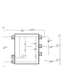
Look at the data sheet block diagram.

It is not in a turned on driving state, just floating high. Measure the voltage between source and gate on the high side, it will be close to 0;
If you load the output in this state, the gate will be pulled low and and only leakage current will flow.

You can turn on the low side now to charge the bootstrap cap. Turning on the low side provides a path for the gate charge on the high side and the high side will be held off.

By running I mean that the inputs are being clocked at a frequency that charges the bootstrap cap and driving a load.
If you scope the output now, it will be working correctly.

Data Sheet

Floating Channels Designed for Bootstrap Operation
to +600V

VS High-Voltage Floating Supply Return
HO High-Side Driver Output
VB High-Side Floating Supply
 
Last edited:

Sorry for re-enabling this post but i think its better than creating a new one!

I am still building this H-bridge and after the creation of the pcb and some failures to run properly the bridge, i decided to look deeper of how things work in my circuit. After some hours studying these two references
**broken link removed** thanks to alexan_e, and
https://www.fairchildsemi.com/an/AN/AN-6076.pdf thanks to.. FAIRCHILD
i have pretty clear image with whats going on with my driver and bootstrap circuit. As i mentioned in my first post, i am trying to drive the motor using this circuit FAN7382.jpg

As i was studying the references i ended up to draw the next picture to fully understand what's going on

FAN7382_bootstrap.jpg

Now, according to my calculations, a CBOOT of 10.1uF is far too big!

Cboot = Qtotal/ΔVboot (1)
where:

ΔVboot = the maximum allowable voltage drop = Vdd - Vf - V_gs.min
where Vdd = 12V
Vf = 0.7V
and lets say the minimum safe gate drive voltage is 11V, so
ΔVboot = 0.3V

Qtotal = Q_gate+ Q_bst + Q_LS (2)
with Qbst = Ibst x Ton and
Ibst = I_lkcap + I_lkGS + I_QBS + I_lk + I_lkdiode

So
Q_gate = 112 nC
Q_LS = 3 nC
Qbst = (170,2 uA x Ton)

If i am correct, the Ton time depends on the switching frequency. Let's assume that my switching frequency will be 33 KHz
(I know that frequency is more than it may be needed but since i'm using the arduino-uno as the uC of my application and unipolar complementary (4-quadrant) PWM switching technique, this frequency is possible for all the three timers of my uC)
So for a 33KHz the time period of the PWM will be 30 usec. That equals to 100% of duty cycle. Now lets assume that i need 95% of duty cycle. That means that the time of 5% of duty cycle(Toff) MUST be enough to charge the Cboot. So i guess for Ton i use 28.5 usec (95% of 30usec) and that gives me

Qtotal = 112 nC + 3 nC + 4.85 nC = 119.85 nC
and therefore
Cboot = Qtotal / ΔVboot = 400 nF

Now how do i know that 5% of duty cycle (Toff = 1.5 usec) is enough time to charge the Cboot??

In slup169.pdf it refers to two extreme operating conditions that must be considered.

The first is talking about when is necessary to keep the main switch/mosfet ON for several switching cycles and gives the equation
Cbst.min = { Qg + Q_LS + ( Ibst x Ton.max) } / ΔVboot
but i think thats not my case as i continuously switch on/off the high and low side

and the second, when is required pulse skipping when the mosfet stays OFF for several switching cyces and gives the equation
Cbst.min = { Qg + ( I_LK,D + I_Q,LS + I_Q,DRV) x Toff.max } / ΔVboot
which i think is my case as i have one driver OFF/OFF in every commutation step, but i don't think is what i need as i want an equation that uses the Toff.min term to be sure that this time is enough to charge my Cboot.

(I guess the big difference between the Cboot exist(10,1uF) in the schematic and the Cboot i calculated so far(400 nF), is because of the different switching frequency i want to use)

Thanks in advanced and sorry for this biiig post!
Dimitris
 

Before considering extreme duty cycles, you should test the circuit in more regular operation. Unfortunately, I'm unable to understand which problems you are actually observing.
 

Thanks for your reply FvM!

I am going to test the circuit with 50% duty cycle (Ton = Toff) tomorrow because i will have access to an oscillator.

I'm not "observing" any problem yet, i just wanted to calculate a bootstrap capacitor value for a minimum Toff time (charging time) for theory and practical reasons!
 

i just wanted to calculate a bootstrap capacitor value for a minimum Toff time (charging time) for theory and practical reasons!
Minimum Toff time respectively duty cycle doesn't primarly depend on the capacitor value, because it's a charge balance problem. Of course, you need to keep a minimum capacitance according to the PWM frequency and acceptable voltage drop. Maximum capacitance is more a matter of inrush current and form factors. The selection didn't yet seem particularly critical to me.
 

Status
Not open for further replies.

Similar threads

Part and Inventory Search

Welcome to EDABoard.com

Sponsor

Back
Top