Continue to Site

Welcome to EDAboard.com

Welcome to our site! EDAboard.com is an international Electronics Discussion Forum focused on EDA software, circuits, schematics, books, theory, papers, asic, pld, 8051, DSP, Network, RF, Analog Design, PCB, Service Manuals... and a whole lot more! To participate you need to register. Registration is free. Click here to register now.

Problem with Charge redistribution DAC

Status
Not open for further replies.

Ravinder487

Full Member level 3
Joined
Jul 9, 2010
Messages
169
Helped
0
Reputation
0
Reaction score
0
Trophy points
1,296
Location
Bangalore, India
Activity points
2,469
Hi all,
I'm facing one serious problem with Charge redistribution DAC

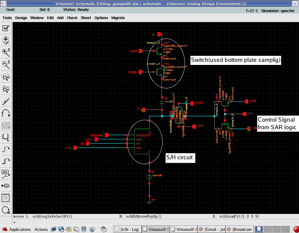
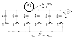
During sampling phase top switch(circled in fig) tries to discharge output of DAC to ground,but in sampling phase all the capacitors are charged to input voltage hence bottom plates of all capacitors track the input signal. Due to this all the top plates(shorted together) are following input signal and aren't getting ground.
I hope you all understood my problem. Please help me solving this issue. What type of switch do I need to use.
 
Last edited:

I've implemented top switch with an NMOS transistor and bottom switches with boot-strapped NMOS transistor.
 

Hi Ravinder,

I am not sure I get the problem:
unless you have negative voltages at play, your NMOS switch is the right choice to discharge the top-plates

as of the bottom plates I have to assume that you are dealing with high voltages if you need to bootstrap that switch

Can you provide the voltage values for the symbols in your schematic (a larger picture would help) and your supplies?
 

This is the schematic of 1bit DAC.
My input signal(voltage source in fig) is sine wave with 600mV dc and 600mV ac and a frequency of 100MHz.
Clk is high during sampling phase,Clkb is inverted version of Clk and Clkboost is clamped(by 1.2) version of Clk.Clkd is advanced(by 40p) version of Clk.
Clkk,Clkkb are high during redistribution phase.
Clk,Clkb,Clkk and Clkkb are pulse voltages with 1.2V as high level and 0 as low level.
 
Last edited:

So -if I am following- this DAC is part of a successive-approximation ADC, it looks very similar to the design on Baker's book (2nd edition page 1006) the only difference I see is that in his schematic he uses the output buffer to reset the top-plate:
the top plate is connected to the inverting input of the comparator and the reset switch (circled in your first schematic) closes the feedback loop to make the comparator into a unit-gain buffer
This topology has the advantage of autozeroing the comparator offset.

In any case whichever option you choose, your initial description is a bit hard to swallow:
- after resetting the top-plate to ground, you begin sampling with the reset switch still closed to ground and release reset only once the bottom plate has a stable sample, right?
- then you ground all bottom plates ang your sample gets pushed to the top plates

Which step fails?
 

Yes but it does not make sense:
if the top of the caps is connected to ground they will not track the input (unless the resistance of the switch is very very high -and this is unlikely)

can you show us a plot of the top plates voltage, input signal, sample and hold output and relevant timing signal (top plate reset and sampling clock)?
 

Consider first two extreme cases:
- if the top plates are connected directly to an ideal source (0 resistance between top cap and ideal 0V source) then by definition their potential is defined by the source and cannot track anything on the bottom plate
- if the opposite is true, that is they are floating (infinite resistance between them and the 0V source) than they will instantaneously track the bottom plate voltage.

Now the intermediate cases:
if we use a large resistance between 0V source the top plates and have a voltage step on the bottom plates (sampling) then the top plates will initially jump to track the voltage but slowly discharge to ground, as you reduce the resistance to ground the time costant of this discharge to ground will become smaller and smaller -and so will the initial voltage bounce- until it is negligible wrt to your timing and you can effectively consider that the top plates are at ideal ground
 
Last edited:
Thanks Dgnani, problem has got solved. I've decreased, increasing its W/L, 'ON' resistance of top switch.Now I'm getting exactly what I needed. Now I get to know that resistance of Top switch should be in comparable to combined resistance of all bottom switches.
 

Thanks for sharing the good news!

Good look with with your design!
 
Status
Not open for further replies.

Part and Inventory Search

Welcome to EDABoard.com

Sponsor

Back
Top