Continue to Site

Welcome to EDAboard.com

Welcome to our site! EDAboard.com is an international Electronics Discussion Forum focused on EDA software, circuits, schematics, books, theory, papers, asic, pld, 8051, DSP, Network, RF, Analog Design, PCB, Service Manuals... and a whole lot more! To participate you need to register. Registration is free. Click here to register now.

Problem when using nDMOS as switches at Charge Pump Design

Status
Not open for further replies.

shenlufei2005

Newbie level 5
Joined
Jan 19, 2010
Messages
8
Helped
0
Reputation
0
Reaction score
0
Trophy points
1,281
Location
Darmstadt
Activity points
1,348
Hello everyone,

I am trapped in the warnings of the simulation under Cadence/Spectre.

Warning from spectre at time = 2.44075 ns during transient analysis `tran'.
WARNING (CMI-2139): M2.m1: The bulk-drain junction current exceeds `imelt'. The results computed by Virtuoso(R) Spectre are now incorrect because the junction current model has been linearized.
WARNING (CMI-2144): M2.m1: The bulk-drain junction current exceeds `imax'.


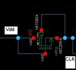
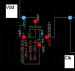
There are uncountable similar warnings and notices during the simulation of the charge pump. Since the bulk and the source of the nDMOS Switch are connected together, the if the output voltage is higher than the input one, the bulk voltage is inevitably higher than the drain voltage. As the consequences, the bulk drain diode will be turned on and the current will be very dangerous for the device.


However, since nDMOS is widely used as switches now, has anybody ever encountered such problems? Are the warnings and notices (no errors) after the simulation of Spectre/Cadence very important??


Many thanks,


Lufei
 

You really don't want the body diode to forward bias,
in a junction isolated technology especially.

You can make a "butterfly" DMOS that has symmetric
high breakdown and float the body center node, at
the cost of more on resistance.
 

Thans for the reply. But my problem is that why there are such warnings. I have tried the both direction. But the warnings are still there.
 

Attachments

  • 1.JPG
    1.JPG
    11.3 KB · Views: 57
  • 3.JPG
    3.JPG
    13.9 KB · Views: 58

... why there are such warnings.
Because the current is too high. Practically a short circuit.

I have tried the both direction. But the warnings are still there.
Of course. You can't use the circuit configuration of the left picture (3.jpg). For this current direction - if you can't separate the bulk connection from the source - you need a 2nd (lateral) MOSFET or the butterfly structure, as d..._freebird advised.
 

Thank you for your advice. But as far as I know, we can use the nDMOS like that in 3.jpg, not using Mos-diode configuration, but just using the bulk/source drain diode as the Switch. ( Plase seee Page 2 in PDF-file in attachment.) Of course, there is large current at the start time at the first stages,,,... but the maximal instant current just about 25 mA, when Vdd= 12V, is it really so large that it exceeds the Imax? I cannot find the maximum rating of this bulk drain current in data sheets, usually not mentioned.

Confused a lot.
 

Attachments

  • A DMOS integrated 320mW capacitive 12V to 70V.pdf
    317 KB · Views: 57

You could look into the model files and see whether you
find the derivation and values for imax, imelt reasonable.
But I don't think you have the data to judge it. It might
be that the values are set very low, to act as a "don't
do that!" for forward biased D-B junction (which stands
a good chance of triggering parasitic devices unless you
are really conservative with ties / guardrings).
 

... just using the bulk/source drain diode as the Switch. ( Plase seee Page 2 in PDF-file in attachment.)
If this is the intention then it's ok.

... is it really so large that it exceeds the Imax? I cannot find the maximum rating of this bulk drain current in data sheets, usually not mentioned.
Try to find this current limit in the nDMOS model which you use. Another chance is to replace the nDMOS by an appropriate standard diode (for your simulation only) and so receive the correct current information.

You may assume that the parasitic bulk/source-drain (reverse) diode is able to stand at least the same current as the max. specified forward current of the nDMOS structure (because of at least the same area).
 

Status
Not open for further replies.

Part and Inventory Search

Welcome to EDABoard.com

Sponsor

Back
Top